PCB board production process
Printed circuit board-inner circuit-pressing-drilling-plated through hole (primary copper)-outer circuit (secondary copper)-solder resist green paint-text printing-contact processing-forming cutting-final inspection packaging.
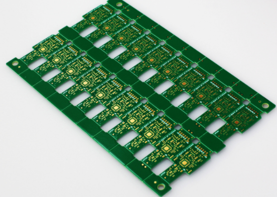
A printed circuit board
In SMT processing, printed circuit boards (Printed Circuit Boards) are a key part. It is equipped with other electronic components and connected to the circuit to provide a stable circuit working environment. For example, the circuit configuration can be divided into three categories:
Single panel: The metal circuit that provides the connection of the parts is arranged on an insulating substrate material, which is also a support carrier for installing the parts.
Double-sided board: When the single-sided circuit is not enough to provide the connection requirements of electronic parts, the circuit can be arranged on both sides of the substrate, and through-hole circuits can be deployed on the board to connect the circuits on both sides of the board.
Multilayer board: In the case of more complex application requirements, the circuit can be arranged in a multilayer structure and pressed together, and through-hole circuits are arranged between the layers to connect the circuits of each layer.

Inner line
The copper foil substrate is first cut into a size suitable for processing and production. Before laminating the substrate, it is usually necessary to properly roughen the copper foil on the surface of the board by brushing, microetching, etc., and then attach the dry film photoresist tightly to it at an appropriate temperature and pressure. Send the dry film photoresist substrate to the UV exposure machine for exposure. The photoresist will undergo polymerization in the light-transmitting area of the negative film after being irradiated by ultraviolet light (the dry film in this area will be affected by the later development and copper etching steps. Keep it as an etching resist), and transfer the circuit image on the negative to the dry film photoresist on the board.
After tearing off the protective film on the film surface, first use sodium carbonate aqueous solution to develop and remove the unlit area on the film surface, and then use a mixed solution of hydrochloric acid and hydrogen peroxide to corrode and remove the exposed copper foil to form a circuit. Finally, the dry film photoresist that has worked well is washed away with sodium hydroxide aqueous solution.
For inner circuit boards with more than six layers (inclusive), an automatic positioning punching machine is used to punch out the riveting reference holes for the alignment of the interlayer circuits. The finished inner circuit board must be bonded with the outer circuit copper foil with glass fiber resin film. Before pressing, the inner layer board needs to be blackened (oxidized) to passivate the copper surface to increase insulation; and the copper surface of the inner layer circuit is roughened to produce good adhesion to the film.
When laminating, first riveting the inner circuit boards of six layers (including) with a riveting machine in pairs. Then use a tray to neatly stack them between the mirror steel plates, and send them into a vacuum laminator to harden and bond the films with proper temperature and pressure. After pressing the circuit board, the target hole is drilled by the X-ray automatic positioning target drilling machine as the reference hole for the alignment of the inner and outer layers. And make appropriate fine cutting of the edge of the board to facilitate subsequent processing.
ipcb is a high-precision, high-quality PCB manufacturer, such as: isola 370hr PCB, high-frequency PCB, high-speed PCB, ic substrate, ic test board, impedance PCB, HDI PCB, Rigid-Flex PCB, buried blind PCB, advanced PCB, microwave PCB, telfon PCB and other ipcb are good at PCB manufacturing.