With the continuous advancement of electronic technology, more and more fields will be applied to embedded systems. Among these many applications, people are no longer considering functions and performance, but reliability and compatibility. Then, how to improve the signal integrity of the embedded system PCB through wiring technology has become an "important issue."
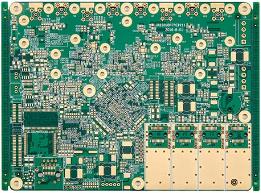
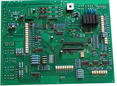
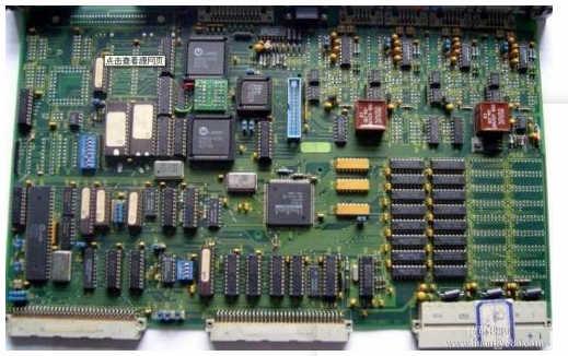
As we all know, PCB (Printed Circuit Board) is the basic support of circuit components and devices in electronic products, and its design quality often directly affects the reliability and compatibility of embedded systems. In the past, in some low-speed circuit boards, the clock frequency was generally only about 10 MHz. The main challenge for circuit board or package design was how to route all signal lines on the double-layer board and how to not damage the package during assembly.
Since the interconnection line never affects system performance, the electrical characteristics of the interconnection line are not important. In this sense, the interconnection lines in the signal low-speed circuit board are smooth and transparent. However, with the development of embedded systems, the circuits used are basically high-frequency circuits. As the clock frequency increases, the rising edge of the signal becomes shorter, and the capacitive reactance and inductance generated by the printed circuit to the passing signal will be much greater than The resistance of the printed circuit itself seriously affects the integrity of the signal. For embedded systems, when the clock frequency exceeds 100 MHz or the rising edge is less than 1 ns, the signal integrity effect becomes important.

In the PCB, the signal line is the main carrier of signal transmission, and the routing of the signal line will directly determine the superiority of the signal transmission, which directly affects the performance of the entire embedded system. Unreasonable wiring will seriously cause a variety of signal integrity problems, and cause timing, noise, and electromagnetic interference (EMI) to the circuit, which will seriously affect the performance of the embedded system. In this regard, this article starts from the actual electrical characteristics of signal lines in high-speed digital circuits, establishes electrical characteristics models, finds the main reasons that affect signal integrity and solutions to problems, and gives attention to the problems in wiring and the methods and techniques to follow. .
Signal integrity
Signal integrity refers to the quality of the signal on the signal line, that is, the ability of the signal to respond with the correct timing and voltage level in the circuit. A signal with good signal integrity means that it has what must be achieved when needed The value of the voltage level. Poor signal integrity is not caused by a single factor, but by multiple factors in board-level design. Signal integrity problems are reflected in many aspects, including delay, reflection, crosstalk, overshoot, oscillation, and ground bounce.
Delay: Delay means that the signal is transmitted at a limited speed on the transmission line of the PCB board. The signal is sent from the sending end to the receiving end, during which there is a transmission delay. The signal delay will affect the embedded timing; the transmission delay mainly depends on the length of the wire and the dielectric constant of the medium around the wire. In a high-speed digital system, the length of the signal transmission line is the most direct factor that affects the phase difference of the clock pulse. The phase difference of the clock pulse refers to the time when the two clock signals generated at the same time arrive at the receiving end are not synchronized. The clock pulse phase difference reduces the predictability of the signal edge arrival. If the clock pulse phase difference is too large, an error signal will be generated at the receiving end.
Reflection: Reflection is the echo of the signal on the signal line. When the signal delay time is much longer than the signal transition time, the signal line must be used as a transmission line. When the characteristic impedance of the transmission line does not match the load impedance, part of the signal power (voltage or current) is transmitted to the line and reaches the load, but part of it is reflected. If the load impedance is less than the original impedance, the reflection is negative; otherwise, the reflection is positive. Variations in wiring geometry, incorrect wire termination, transmission through connectors, and discontinuities in the power plane can all cause such reflections.
Crosstalk: Crosstalk is the coupling between two signal lines, and the mutual inductance and mutual capacitance between the signal lines cause noise on the signal line. Capacitive coupling induces coupling current, and inductive coupling induces coupling voltage. Crosstalk noise originates from electromagnetic coupling between signal wire networks, between signal systems and power distribution systems, and between vias. Cross-winding may cause false clocks, intermittent data errors, etc., which may affect the transmission quality of adjacent signals. In reality, crosstalk cannot be completely eliminated, but it can be controlled within the range that the system can withstand. The parameters of the PCB layer, the signal line spacing, the electrical characteristics of the driving end and the receiving end, and the baseline termination method all have a certain impact on the crosstalk.
Overshoot and undershoot: Overshoot is the first peak or valley value that exceeds the set voltage. For rising edges, it refers to the highest voltage; for falling edges, it refers to the lowest voltage. Undershoot means that the next valley or peak value exceeds the set voltage. Excessive overshoot can cause the protection diode to work, leading to its premature failure. Excessive undershoot can cause false clock or data errors (misoperation).
Oscillation and ring oscillation: Oscillation phenomena are repeated overshoot and undershoot. The signal oscillation is the oscillation caused by the inductance and capacitance of the line transition, which belongs to the under-damped state, and the surrounding oscillation belongs to the over-damped state. Oscillation and surround oscillation are also caused by many factors like reflection. Oscillation can be reduced by proper termination, but it is impossible to completely eliminate it.
Ground bounce noise and return noise: When there is a large current surge in the circuit, it will cause ground bounce noise. For example, when a large number of chip outputs are turned on at the same time, there will be a large transient current between the chip and the board. If the power plane flows through, the inductance and resistance of the chip package and the power plane will cause power noise, which will produce voltage fluctuations and changes on the real ground plane, and this noise will affect the actions of other components. The increase of the load capacitance, the decrease of the load resistance, the increase of the ground inductance, and the increase of the number of switching devices will all lead to the increase of the ground bounce.
Analysis of electrical characteristics of transmission channel
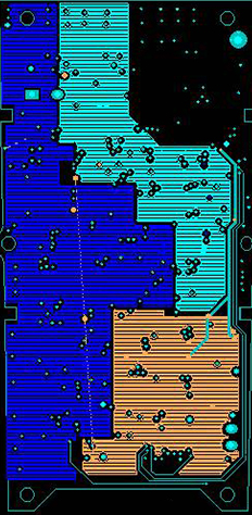
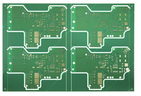
In a multilayer PCB, most of the transmission lines are not only arranged on a single level, but staggered on multiple levels, and each level is connected through vias. Therefore, in a multilayer PCB, a typical transmission channel mainly includes three parts: a transmission line, a wiring corner, and a via. In the case of low frequencies, printed lines and trace vias can be regarded as ordinary electrical connections to connect the pins of different devices, which will not have much impact on signal quality. However, in the case of high frequency, the printed lines, corners and vias should not only consider their connectivity, but also the influence of their electrical characteristics and parasitic parameters at high frequencies.
Analysis of electrical characteristics of transmission lines in high-speed PCB
In high-speed PCB design, it is inevitable to use a large number of signal connection lines, and their lengths are different. The delay time of the signal passing through the connection line cannot be ignored compared with the change time of the signal itself. The signal is on the connection line at the speed of electromagnetic waves. For transmission, the connecting line at this time is a complex network with resistance, capacitance, and inductance, which needs to be described by a distributed parameter system model, that is, a transmission line model.
The transmission line is used to transmit the signal from one end to the other. It consists of two wires with a certain length, one is called the signal path, and the other is called the return path. In low-frequency circuits, the characteristics of the transmission line appear as purely resistive electrical characteristics. In a, as the frequency of the transmission signal increases, the capacitive impedance between the wires decreases, and the inductive impedance on the wires increases. The signal wire will no longer only be a pure resistance, that is, the signal will not only be transmitted on the wire, but also Will propagate in the medium between conductors. If the signal frequency is further increased, when jωL>>R,1/(jωC)