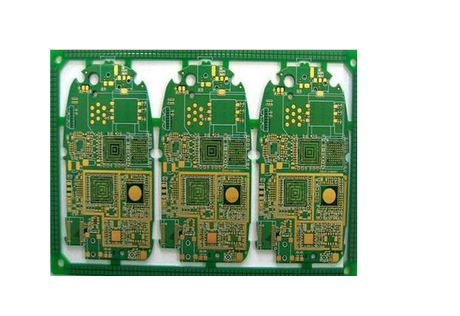
As HDI board meets the requirements of the development of high-integration IC and high-density interconnection assembly technology, it pushes PCB manufacturing technology to a new level, and has become one of the biggest hotspots of PCB manufacturing technology! In the CAM production of various PCBs, People engaged in CAM production agree that HDI mobile phone boards have complex shapes, high wiring density, and CAM production is difficult, and it is difficult to complete them quickly and accurately! Faced with the requirements of customers for high quality and fast delivery, I continue to practice and summarize, I have a little bit of this, and I would like to share it with fellow CAM colleagues.
1. How to define SMD is the first difficulty in CAM production
In the PCB production process, graphics transfer, etching and other factors will affect the final graphics. Therefore, we need to compensate the lines and SMD separately according to the customer's acceptance criteria in the CAM production. If we do not define the SMD correctly, parts of the finished product may appear SMD is too small. Customers often design 0.5mm CSP in HDI mobile phone boards. The pad size is 0.3mm, and some CSP pads have blind holes. The corresponding pads of the blind holes are also 0.3mm, making the CSP pads and blind holes The corresponding pads of the holes overlap or cross each other. In this case, you must operate carefully to prevent errors. (Take genesis2000 as an example)

Specific production steps:
1. Close the drilling layer corresponding to the blind hole and buried hole.
2. Define SMD
3. Use the FeaturesFilterpopup and Referenceselectionpopup functions to find the pads of the include blind holes from the top layer and the bottom layer, respectively, the moveot layer and the b layer.
4. Use the Referenceselectionpopup function on the t layer (the layer where the CSP pad is located) to select the 0.3mm pad that touches the blind hole and delete it. The 0.3mm pad in the CSP area of the top layer is also deleted. Then according to the customer design CSP pad size, location, number, make a CSP and define it as SMD, then copy the CSP pad to the TOP layer, and add the pad corresponding to the blind hole on the TOP layer. b-layer similar method
5. Find out other SMDs with missing definitions or multiple definitions based on the profile provided by the customer.
Compared with the conventional production method, the purpose is clear, the steps are few, this method can avoid misoperation, fast and accurate!
2. Removing non-functional pads is also a special step in HDI mobile phone boards
Taking the ordinary eight-layer HDI as an example, first remove the non-functional pads corresponding to the through holes in the 2-7 layers, and then remove the non-functional pads corresponding to the 2-7 buried holes in the 3-6 layers. Functional pad.
Proceed as follows:
1. Use the NFPRemovel function to remove the corresponding pads of the top and bottom layers of non-metallized holes.
2. Close all drilling layers except through holes, select NO for RemoveundrilLEDpads in the NFPRemovel function, and remove 2-7 layers of non-functional pads.
3. Close all drilling layers except the buried holes of layer 2-7, select NO for Removeundrilledpads in the NFPRemovel function, and remove the non-functional pads of layer 3-6.
Using this method to go to non-functional pads, the idea is clear, easy to understand, and it is most suitable for people who are just engaged in CAM production.
C. About laser drilling
The blind holes of HDI mobile phone boards are generally micro-holes of about 0.1mm. Our company uses CO2 lasers. Organic materials can strongly absorb infrared rays. Through the thermal effect, the holes are ablated, but the absorption rate of copper to infrared rays is very small. The melting point of copper is high, and CO2 laser cannot ablate copper foil, so the "conformalmask" process is used to etch the copper skin of laser drilling holes with etching solution (CAM needs to make exposure film). At the same time, in order to ensure that there is a copper skin in the secondary outer layer (the bottom of the laser hole), the distance between the blind hole and the buried hole must be at least 4mil or more. For this reason, we must use Analysis/Fabrication/Board-Drill-Checks to find out the unsatisfactory conditions的孔位. The hole position.
4. Plug hole and solder mask
In the HDI laminated configuration, the secondary outer layer is generally made of RCC material, which has a thin medium thickness and low glue content. The process experimental data shows that if the thickness of the finished plate is greater than 0.8mm, the metallization groove is greater than or equal to 0.8mmX2.0mm, One of the three metalized holes is greater than or equal to 1.2mm, two sets of plug hole files must be made. That is, the holes are plugged twice, the inner layer is flattened with resin, and the outer layer is directly plugged with solder mask ink before the solder mask. During the solder mask manufacturing process, there are often vias that fall on or next to the SMD. The customer requires all vias to be plugged, so when the solder mask is exposed or exposed by half of the hole, it is easy to leak oil. CAM staff must deal with this. Under normal circumstances, we prefer to remove the via. If the hole cannot be removed, follow the steps below:
1. Add a 3MIL light transmittance point smaller than the finished hole on the solder mask to the via hole position covered by the solder mask.
2. Add a 3MIL larger light-transmitting point than the finished hole on the solder mask layer to the via hole position of the solder mask opening touch. (In this case, the customer allows a small amount of ink on the pad)
Five. Shape making
HDI mobile phone boards are generally delivered by jigsaw, with complex shapes, and the customer attaches a CAD drawing of the jigsaw. If we use genesis2000 to draw according to the customer's drawing, it is quite troublesome. We can directly click the "Save As" in the CAD format file *.dwg to change the save type to "AutoCADR14/LT98/LT97DXF(*.DXF)" and then read the *.DXF file in the normal way of reading the genber file . While reading the shape, the size and position of the stamp hole, positioning hole and optical positioning point are also read, which is fast and accurate.
6. Milling frame processing
When processing the milled outline frame, unless the customer requires the copper to be exposed during the CAM production, in order to prevent the copper from turning over the edge of the board, according to the production specification, it is required to cut a little copper in the frame. If the two ends of A are not in the same network, and the copper The width of the skin is less than 3mil (may not be able to make graphics), which will cause an open circuit. No such problems can be seen in the analysis report of genesis2000, so we must find another way. The PCB factory can do one more network comparison, and in the second comparison, the copper of the frame will be cut 3mil into the board. If the comparison result is not open, it means that both ends of A belong to the same network or the width is greater than 3mil. Make graphics). If there is an open circuit, widen the copper sheet.