PCB, the PrintedCircuitBoard printed circuit board, is not only the support of electronic components, but also the carrier of electrical connection of electronic components. Before the advent of PCB, the connection between electronic components was completed by direct connection of wires; but now, the wire connection method is only used in laboratory tests, and PCB has occupied an absolute control position in the electronics industry.
talk about history, the past and present of PCB
The development history of PCB can be traced back to the early 20th century. In 1936, Austrian Paul Eisler (Paul Eisler) applied PCB in the radio, putting PCB into practical use for the first time; in 1943, the United States widely used the technology in military radios; in 1948, the United States officially recognized that the invention can be used business use. As a result, PCB began to be widely used since the mid-1950s, and then entered a period of rapid development.

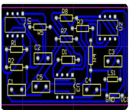
As PCBs become more and more complex, when designers use development tools to design PCBs, it is easy to confuse the definition and purpose of each layer. When our hardware developers draw the PCB by themselves, it is easy to cause unnecessary misunderstandings in production because they are not familiar with the purpose of each layer of the PCB. In order to avoid this situation, take AltiumDesignerSummer09 as an example to classify and introduce each PCB layer.
The difference between PCB layers
Signal Layer (SignalLayers)
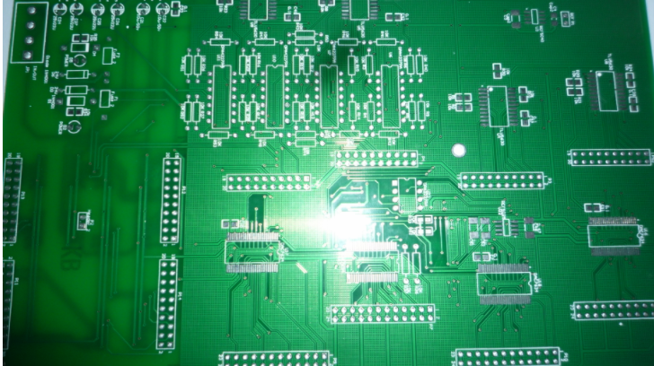
AltiumDesigner can provide up to 32 signal layers, including the top layer (TopLayer), bottom layer (BottomLayer) and middle layer (Mid-Layer). The layers can be interconnected through vias (Via), blind vias (BlindVia) and buried vias (BuriedVia).
1. The top signal layer (TopLayer)
is also called component layer, which is mainly used to place components. For double-layer boards and multilayer boards, it can be used to arrange wires or copper.
2, the bottom signal layer (BottomLayer)
is also called soldering layer, which is mainly used for wiring and soldering. For double-layer boards and multilayer boards, it can be used to place components.
3, the middle signal layer (Mid-Layers)
can have up to 30 layers. It is used to arrange signal lines in a multi-layer board. Power lines and ground lines are not included here.
Internal Planes
is usually abbreviated as the inner electric layer, which only appears in multilayer boards. The number of PCB board layers generally refers to the sum of the signal layer and the inner electric layer. Same as the signal layer, the inner electric layer and the inner electric layer, and the inner electric layer and the signal layer can be connected to each other through through holes, blind holes and buried holes.
SilkscreenLayers
A PCB board can have up to 2 silk screen layers, namely the top silk screen layer (TopOverlay) and the bottom silk screen layer (BottomOverlay), generally white, mainly used to place printed information, such as component outlines and annotations, various notes Characters, etc., to facilitate the soldering of PCB components and circuit inspection
1, the top silk screen layer (TopOverlay)
is used to mark the projection outline of the component, the label of the component, the nominal value or model, and various annotation characters.
2, bottom silk screen layer (BottomOverlay)
is the same as the top silk screen layer, if all the marks on the top silk screen layer are included, the bottom silk screen layer can be closed.
MechanicalLayers
Mechanical layer is generally used to place indicative information about board manufacturing and assembly methods, such as PCB dimensions, size markings, data materials, via information, assembly instructions and other information. This information varies according to the requirements of the design company or PCB manufacturer. The following examples illustrate our common methods.
Mechanical1: Generally used to draw the frame of the PCB as its mechanical shape, so it is also called the shape layer;
Mechanical2: We used to place the PCB processing process requirement form, including information such as size, plate, and layer;
Mechanical13&Mechanical15: The body size information of most components in the ETM library, including the three-dimensional models of the components; for the sake of simplicity of the page, this layer is not displayed by default;
Mechanical16: The footprint information of most components in the ETM library can be used to estimate the PCB size in the early stages of the project; for the simplicity of the page, this layer is not displayed by default, and the color is black.
MaskLayers
AltiumDesigner provides two types of mask layers (SolderMask) and solder paste layer (PasteMask), in which there are top and bottom layers respectively.