In the ceramic circuit board processing and PCB production process, laser processing mainly includes laser drilling and laser cutting.
Ceramic materials such as alumina and aluminum nitride have the advantages of high thermal conductivity, high insulation and high temperature resistance, and have a wide range of applications in the fields of electronics and semiconductors. However, ceramic materials have high hardness and brittleness, and its molding and processing are very difficult, especially the processing of micropores. Due to the high power density and good directivity of the laser, lasers are generally used to perforate ceramic plates. Laser ceramic perforation generally uses pulsed lasers or quasi-continuous lasers (fiber lasers). The laser beam is focused on On the workpiece placed perpendicular to the laser axis, a laser beam with high energy density (105-109w/cm2) is emitted to melt and vaporize the material. An air stream coaxial with the beam is ejected by the laser cutting head to remove the melted material from The bottom of the incision is blown out to gradually form a through hole.

Due to the small size and high density of electronic devices and semiconductor components, the precision and speed of laser drilling are required to be high. According to the different requirements of component applications, electronic devices and semiconductor components have small size and high density. Due to its characteristics, the precision and speed of laser drilling are required to be high. According to the different requirements of component applications, the diameter of the micro-hole is in the range of 0.05 to 0.2 mm. For lasers used for ceramic precision processing, generally the focal spot diameter of the laser is less than or equal to 0.05mm. Depending on the thickness and size of the ceramic plate, it is generally possible to control the defocus to achieve through-hole punching of different apertures. For through-holes with a diameter less than 0.15mm, Punching can be achieved by controlling the defocus amount.
There are mainly two types of ceramic circuit board cutting: waterjet cutting and laser cutting. Currently, fiber lasers are mostly used for laser cutting on the market. Fiber laser cutting ceramic circuit boards has the following advantages:
(1) High precision, fast speed, narrow cutting seam, small heat-affected zone, smooth cutting surface without burrs.
(2) The laser cutting head will not touch the surface of the material and will not scratch the workpiece.
(3) The slit is narrow, the heat-affected zone is small, the local deformation of the workpiece is extremely small, and there is no mechanical deformation.
(4) The processing flexibility is good, it can process any graphics, and it can also cut pipes and other special-shaped materials.
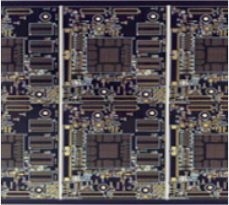
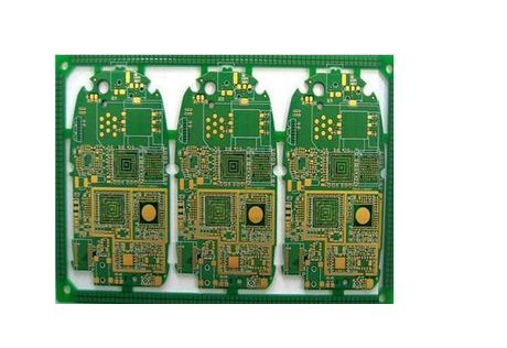
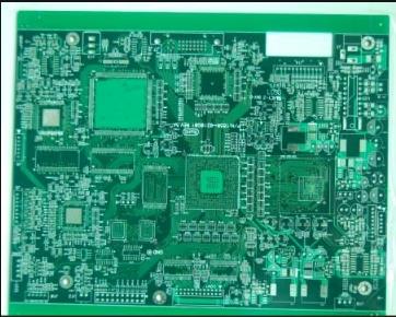
With the continuous advancement of 5G construction, industrial fields such as precision microelectronics and aviation and ships have been further developed, and these fields cover the application of ceramic substrates. Among them, the ceramic substrate PCB has gradually obtained more and more applications due to its superior performance.
Ceramic substrate is the basic material of high-power electronic circuit structure technology and interconnection technology, with compact structure and certain brittleness. In the traditional processing method, there is stress during the processing, and it is easy to produce cracks for the thin ceramic sheets.
Under the development trend of light and thin, miniaturization, etc., the traditional cutting processing method has not been able to meet the demand due to the insufficient precision. Laser is a non-contact processing tool, which has obvious advantages over traditional processing methods in cutting process, and plays a very important role in the processing of ceramic substrate PCB.
With the continuous development of the microelectronics industry, electronic components are gradually developing in the direction of miniaturization, lightness and thinning, and the requirements for precision are getting higher and higher. This is bound to put higher and higher requirements on the processing degree of ceramic substrates. From the perspective of development trend, the application of laser processing ceramic substrate PCB has broad development prospects!