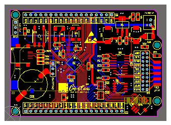
The line drawn by TopLayer (top layer) is red, which is the upper layer of a general double-sided board, and this layer is not used for a single-sided board.
The line drawn by BottomLayer (bottom layer) is blue, which is the line layer above the single panel.
MidLayer1 (MidLayer1) This is the first middle layer. It seems to have 30 layers. Generally, designers can't use it. You don't need to worry about it. It is used when there are multiple panels. The default is not displayed in 99SE, and it is not used.
Mechanical Layers (purple red) are used to mark the size and the board description, which is ignored during the PCB copy board processing, that is, the board is invisible when it is made, and it means simple point annotation.
Top Overlay (the top silk screen layer) (yellow) is the characters on the front of the board. This layer of characters can be used for the TopLayer (top layer) single panel. The Bottom Overlay (bottom screen layer) (brown) corresponds to the BottomLayer (bottom layer), which is the board. For the characters on the back, the above two layers of characters are used when double-sided.
KeepOutLayer (prohibited wiring layer) (purple red with the mechanical layer) is simply the frame and appearance of the board.
Multi layer (multi-layer) (silver) All wiring layers are included. Generally, single and double-sided plug-in pads are on this layer, and the stripes are drawn on all layers.
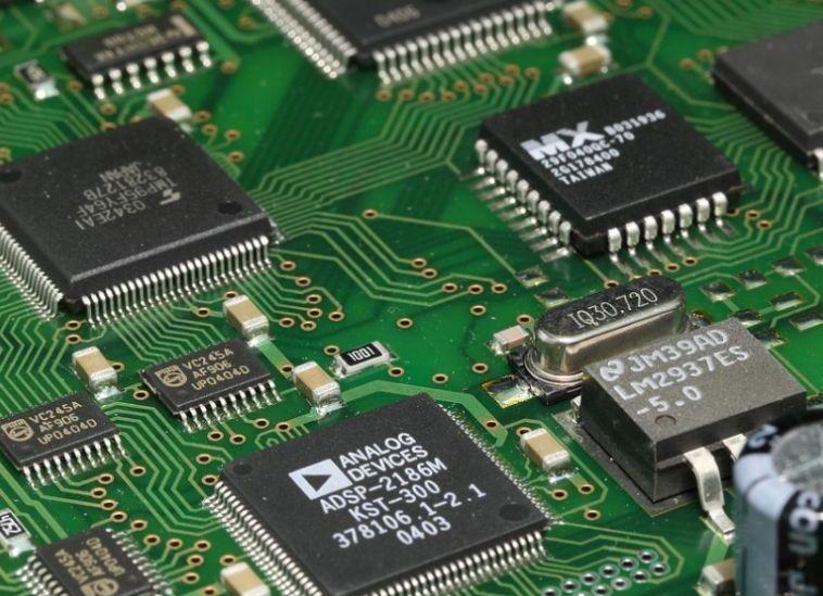
1. TopLayer (top layer) The top layer wiring layer, used to draw electrical connections between components.
2. BottomLayer (bottom layer) bottom wiring layer, which functions as the top wiring layer.
3.MidLayer1 (MidLayer1) is used to draw electrical connection lines on this layer when making multilayer boards, but the cost of multilayer boards is relatively high.
4. Mechanical Layers (mechanical layers) can be used to draw the shape of the PCB printed board, and the parts that need to be dug, and can also be used to annotate the PCB size, etc., can be used to draw the shape of the PCB printed board, and the parts that need to be dug, pay attention Do not use the same mechanical layer for PCB shape, cutouts and PCB annotation dimensions. For example, mechanical layer 1 is used to draw the PCB shape and cutouts, and mechanical layer 13 is used to annotate dimensions. After separation, the technicians of the printed board manufacturer will follow Analyze the things in this layer by yourself whether you need to make this layer.
5. Top Overlay (the top silk screen layer) (yellow) is the characters on the front of the board. This layer of characters can be used for the TopLayer (top layer) single panel. Bottom Overlay (the bottom silk screen layer) (brown) corresponds to BottomLayer (bottom layer). It is the characters on the back of the board. The above two layers of characters are used when double-sided.

6. KeepOutLayer (forbidden wiring layer) is used to draw the prohibited wiring area. If there is no mechanical layer drawn on the printed board, the people of the printed board manufacturer will treat this layer as the PCB shape. If both the KEEPOUT LAYER layer and the mechanical layer are used, the default is to use the mechanical layer as the PCB shape, but the technicians of the printed board manufacturer will distinguish it by themselves, but if they can’t distinguish it, they will default to the mechanical layer. Shape layer.
7. Multi layer (multi-layer) (silver) All wiring layers are included. Generally, single and double-sided plug-in pads are on this layer, and the stripes are drawn on all layers.
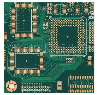
One, Signal Layers (signal layer)
Protel98 and Protel99 provide 16 signal layers: Top (top), Bottom (bottom) and Mid1-Mid14 (14 middle layers).
The signal layer is the wiring layer used to complete the copper foil traces of the printed circuit board. When designing a double-sided board, generally only two layers of Top (top) and Bottom (bottom) are used. When the number of printed circuit boards exceeds 4 layers, Mid (middle wiring layer) is required.
Two, Internal Planes (internal power supply / ground plane)
Protel98 and Protel99 provide Plane1-Plane4 (4 internal power/ground planes). The internal power/grounding layer is mainly used for printed circuit boards with more than 4 layers as the dedicated wiring layer for power and grounding, and the double-sided board does not need to be used.
Three, Mechanical Layers (mechanical layer)
The mechanical layer is generally used to draw the frame (boundary) of the printed circuit board, usually only one mechanical layer is used. There are Mech1-Mech4 (4 mechanical layers).
4, Drkll Layers (drilling position layer)
has 2 layers: "Drill Drawing" and "Drill Guide". Used to draw the hole diameter and positioning of the hole.
5, Solder Mask (solder mask)
has 2 layers: Top (top layer) and Bottom (bottom layer). The solder mask is drawn on the protective area around the pads and vias on the printed circuit board.
6, Paste Mask (Solder Paste Protective Layer)
has 2 layers: Top (top layer) and Bottom (bottom layer). The solder paste protective layer is mainly used for printed circuit boards with surface-mounted components. At this time, it is required for the installation process of surface-mounted components, and this layer is not required when there are no surface-mounted components.
7, Silkscreen (silk screen layer)
has 2 layers: Top (top layer) and Bottom (bottom layer). The silk screen layer is mainly used to draw text descriptions and graphic descriptions, such as the contours, labels and parameters of components.
8, Other (other layers)