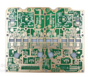
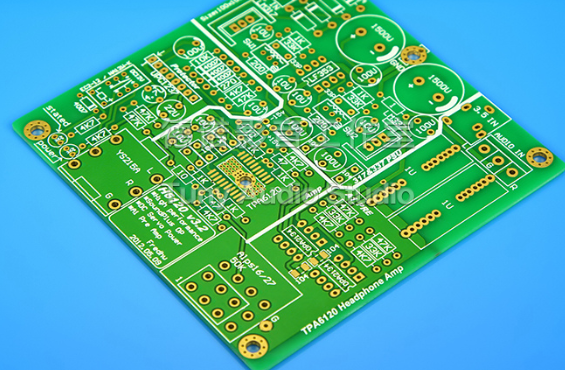
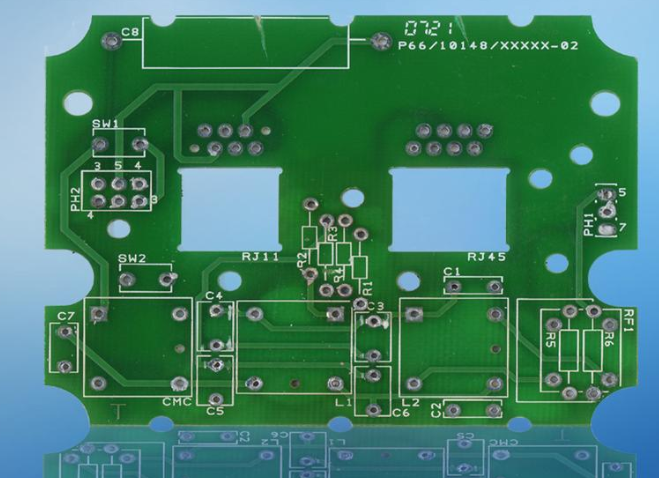
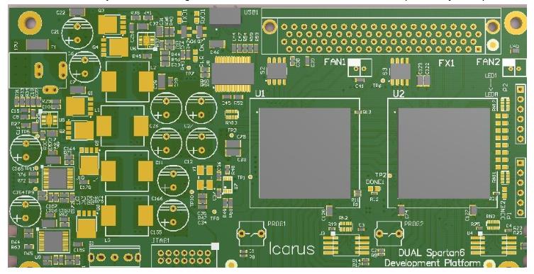
PCB manufacturing is not a simple process. It has many separate components to manage and process. The lack of a component may delay the entire production of the PCB, and may even cost you money. One of the most important components is the Gerber file, which basically describes the layout, layers, design, solder mask, etc. of the PCB. Gerber files help PCB manufacturing. Here, we will discuss seven common mistakes about Gerber files that can delay your PCB production and how you can avoid them.
1: Missing aperture list:
The aperture list contains a description of the shape and size of the tools used to create pads and tracks. The Gerber file should contain a list of individual apertures for all layers, rather than separate ones. It is best not to modify the aperture list output by the software. When using the 274X format, the aperture list is included in the Gerber file. If you use the 274D format, remember that the layout package will also output the aperture list. Some extensions, including .rep, .apt, and .apr. 274D files require manual input of aperture definitions.
2: Excellon drilling file is missing:

Excellon drilling files are used to drive CNC drilling and milling machine tools in PCB manufacturing. They determine where to drill the size. Tool information can also be specified in the drill file or separately. Both gold-plated and non-plated holes are included in a drilling file. It should be in ASCII (odd/none) format, should have 2.4 trailing zero suppression, imperial units, and no steps or repetitions.
3: List of missing tools:
Tool list is basically used in conjunction with Excellon drill file. The drill file will specify the placement of the hole, and the tool list specifies the tool to be used. As mentioned earlier, you can embed the tool list in the Excellon drill file or send it separately. If you use the tool list provided on the production drawing, it is likely to increase the possibility of error. Remember, if your layout software outputs Excellon drill files, it will also output a list of tools, with extensions including .tol and .rep.
4: The Gerber file is missing:
Yes, this is also a common mistake. Gerber files are the most important part of PCB manufacturing. PCBs cannot be manufactured without them. Your Gerber file can be in 274X or 274D format, and English units are preferred. Some manufacturers can also convert your files from other formats to Gerber format. For this, you should check the company's requirements before placing an order.
5: Insufficient annular ring:
The annulus is the area surrounding the through hole on the pad. The width of the annular ring is important because a proper annular width length means good electrical conductivity between the pad and the hole. For example, a .030" pad with a .020" hole will have a .005" ring ring width. For manufacturing, we usually use the smallest .005" ring ring for through holes or at least .007" for component holes In order to maintain proper copper spacing, you should set enough annular rings in the layout software.
6: Insufficient copper trace width/spacing:
The copper pitch is the minimum pitch or air gap between two adjacent copper features, and the trace width is the minimum width of the copper trace. You should keep the minimum .005" trace width/spacing. Layout packages usually check this as a DFM (Design for Manufacturability) check. You should always set sufficient trace width and spacing in the layout software.
7: Insufficient clearance inside PCB:
The PCB internal gap is the minimum distance from the edge of the hole to any surrounding unconnected internal copper layers. Providing sufficient internal clearance helps to ensure that the drilling does not cause any short circuits in the internal copper layer. This is important for both plated and unplated holes. The preferred internal clearance is 0.015 inches, and the minimum internal clearance should not be less than .010 inches.