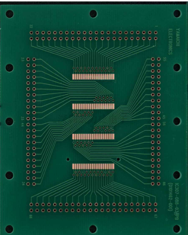
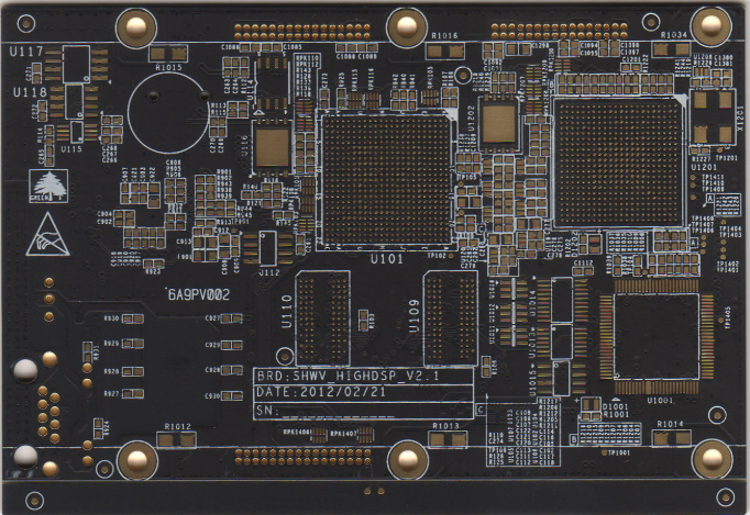
Although there are many disputes about the value, definition, variability, and technology of design for manufacturability (DFM), all problems are based on chips. Of course, when we start to consider 45 and 32 nanometer designs, chip DFM is a critical requirement. However, the focus on chip DFM has overlooked a more important technical need: DFM for printed circuit boards.
We all know that even if the silicon chip is 100% perfect, if any component of the chip-to-chip communication link (such as package, connector or circuit board) is damaged, the target system may still not work properly. Many packaging, connector, and PCB suppliers may be driven by system designers to control their processing tolerances.
However, unless all suppliers unanimously strengthen the specifications, for example, a connector with a tolerance of plus or minus 5% may not be effective for a system with a tolerance of plus or minus 10% on the PCB. In order to optimize system design, designers need to study the causality of each component. So far, we have no DFM tools to deal with design issues such as these.

In the pre-layout design stage, high-speed system or signal integrity engineers usually can only perform limited Spice simulations. In order to ensure that the system works normally, it is necessary to simulate the boundary conditions that can cover all the machining tolerances.
For example, changes in metal line width, dielectric stack height, dielectric constant, and loss tangent within the PCB can all affect impedance and attenuation. However, only engineers in larger companies may have the resources to customize their own scripts to perform thousands of simulation tasks and then process the results. Even so, there is still no well-defined standard for which variables to scan.
The most obvious lack is the boundary model of the package and the connector. For high-speed designs, these models can only be precisely defined by frequency-related S-parameters. However, very few suppliers provide good S-parameter models, let alone boundary models over a wide range of frequencies.
In the post-layout verification stage, precise extraction and simulation of complex PCBs are required to calculate detailed corners and bends. However, almost no tools are available.
Obviously, a common PCB design and verification method is needed. So, what do we need?
Let us focus on two major areas. For pre-layout design, for example, it is better to have a GUI-driven wiring diagram input editor, so that the designer can easily input the changes of each component, simulate and process the results, and report the generation and impact of each variable.
For post-layout verification, DFM tools need to be able to automatically adjust the layout to cover the boundary conditions, use a fast full-wave extractor to extract parasitic parameters, and use I/O transistor boundary models in circuit simulation.
Only when designers consider work tolerances in design and verification, can they say that they have done design for manufacturability. Only when the tool supplier recognizes that the chip is only a sub-system-such as a part of the PCB, then DFM can ultimately be truly relevant to the customer who develops the end product.
DFM is mainly to study the relationship between the physical characteristics of the product itself and the various parts of the manufacturing system, and use it in product design to integrate the entire PCB manufacturing system for overall optimization and make it more standardized to reduce Cost, shorten production time, improve product manufacturability and work efficiency.