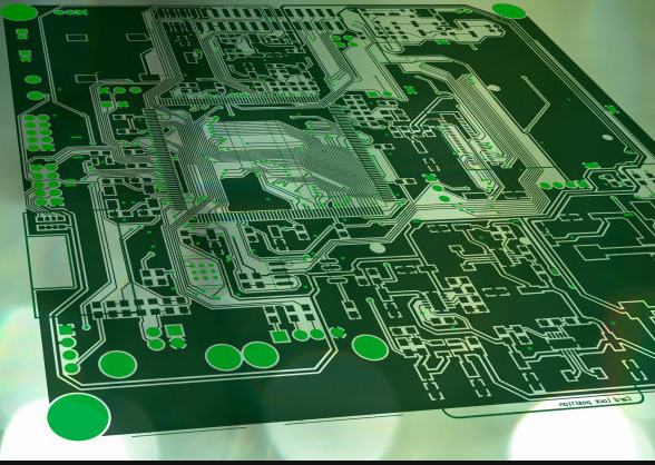
1. The purpose of PCB design should be clear. For important signal lines, the length of the wiring and the processing of the ground loop should be very strict. For low-speed and unimportant signal lines, it can be placed on a slightly lower wiring priority. . The important parts include: power supply division; memory clock line, control line and data line length requirements; high-speed differential line wiring and so on. In the project A, a memory chip is used to implement a 1G DDR memory. The wiring for this part is very critical. It is necessary to consider the topological distribution of the control line and the address line, the length difference control of the data line and the clock line, etc., in the realization In the process, according to the chip's data manual and the actual operating frequency, specific wiring rules can be drawn. For example, the length of the data lines in the same group cannot exceed how many mils, and the difference in length between each channel cannot exceed how many mil and so on. When these requirements are determined, PCB designers can be clearly required to implement them. If all the important wiring requirements in the design are clear, they can be converted into overall wiring constraints, and the automatic wiring tool software in CAD can be used to realize the PCB design. It is also a development trend inhigh-speed PCB design.

2, check and debug
When you are ready to debug a board, you must first make a careful visual inspection to check if there are any visible short-circuits and pin tinning faults during the soldering process, and check if there are any component types that are placed incorrectly, the first pin Put the wrong place, miss the assembly and other problems, and then use a multimeter to measure the resistance of each power supply to the ground to check whether there is a short circuit. This good habit can avoid damaging the board after rashly powering on. You must have a peaceful mind during the debugging process. It is very normal to encounter problems. What you need to do is to do more comparisons and analysis, gradually eliminate possible causes, and firmly believe that "all things can be solved" and "the problem is certain." There is a reason", so that the debugging will be successful in the end.
3, Some summary words
From a technical point of view, every design can finally be made, but the success of a project depends not only on the technical realization, but also closely related to the completion time, the quality of the product, and the cooperation of the team. Therefore, good teamwork, transparent and candid project communication, meticulous and thorough R&D arrangements, and abundant materials and personnel arrangements can ensure the success of a project.A good hardware engineer is actually a project manager. He/she needs to communicate with the outside world to obtain the requirements for his own design, and then summarize and analyze it into a specific hardware implementation. It is also necessary to contact many chip and solution suppliers to select suitable solutions. When the schematic diagram is completed, he/she should organize colleagues to conduct cooperative review and inspection, and work with CAD engineers to complete the PCB design. . At the same time, prepare the BOM list, start purchasing and preparing materials, and contact the processing manufacturer to complete the board placement. During the debugging process, he/she should organize a software engineer to work together to research and debug, cooperate with the test engineer to solve the problems found in the test, and wait until the product is launched to the site. If there is a problem, it needs to provide timely support. Therefore, to be a hardware designer, you must develop good communication skills, the ability to adjust to pressure, the coordination and decision-making ability to handle multiple tasks at the same time, and a good peace of mind. There is also carefulness and seriousness, because a small negligence in the hardware design will often cause very large economic losses. For example, when the PCB design is complete and the manufacturing file is completed, the wrong operation of a board has caused the power layer and the ground layer to be connected. At the same time, after the PCB board was manufactured, it was directly mounted on the production line without inspection. The short circuit problem was discovered during the test, but the components have been soldered to the board, resulting in hundreds of thousands of losses. Therefore, careful and serious inspection, responsible testing, and unremitting learning and accumulation can make a hardware designer make continuous progress, and then the technical industry will achieve a small success.