The process of high-density interconnect build-up PCB multilayer board is the product of the "light, thin, short, small" and multifunctional layer of electronic products. Relevant data reports have some clearer introductions in terms of technical indicators:
1) The aperture of the micro vias (including blind holes and buried holes) is ≤Φ0.1mm; the ring is ≤0.25 mm; 2) the hole density of the micro vias is ≥600 holes/square inch; the wire width spacing is ≤0.10 mm ; 4) The wiring density (set the channel grid as 0.05 inches) exceeds 117 inches per square inch. From the technical indicators, the use of micro-via technology is a practical technical approach to achieve high-density PCBs. Therefore, its classification is often divided according to the formation process of micro vias:
Photoinduced hole forming multilayer multilayer board process
Plasma etch hole manufacturing multilayer multilayer board process
Jet-blasting process for forming holes and build-up multi-layer boards
Laser hole forming multilayer multilayer board process
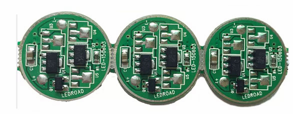
There are three other commonly used classifications for high-density interconnect multilayer multilayer boards. One is divided into the types of dielectric materials of multilayer multilayer boards: 1) Use photosensitive materials to make multilayer multilayer boards, 2) Use Non-photosensitive materials are used to manufacture multi-layer laminates. The second is classified according to the electrical interconnection method: 1) Plating method of micro-via interconnection build-up multilayer boards, 2) conductive adhesive method of micro-via interconnection build-up multilayer boards. The third is to classify according to "core board": 1) "core board" structure, 2) no "core board" structure (the coreless board structure is a high-density interconnection multilayer multilayer board manufactured on a prepreg using special technology) . The high-density interconnect multilayer multilayer board was the first Japanese IBM company published in 1991 the research results of the "surface thin-layer circuit multilayer board" manufacturing technology developed over several years, and it first began to be used in notebook computers. Nowadays, applications on mobile phones and laptops are very popular. It is easier to understand the basic technology and basic process of PCB from the combination of the classification and name of PCB.

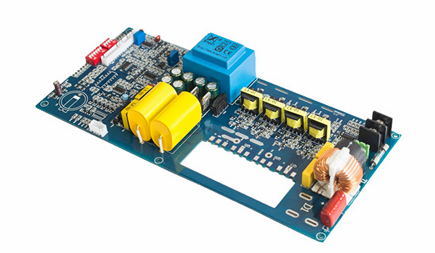
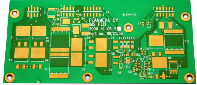
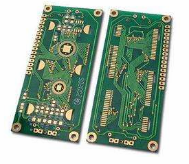
For now, the Computer City is a more intuitive and fully open place where you can see PCB and its applications. Common computer boards are basically printed circuit boards based on epoxy resin glass cloth (because the laptop is a complete machine, it is more It is difficult to see high-density interconnect multilayer multilayer boards), one side of which is the insertion component and the other side is the component pin soldering surface. It can be seen that the solder joints are very regular. The discrete soldering surface of the component legs of these solder joints is called it. For the pad. Why are other copper wire patterns not tinned? Because in addition to the soldering pads and other parts, the surface of the remaining parts has a layer of solder mask resistant to wave soldering. Most of the solder mask on the surface is green, and a few use yellow, black, blue, etc., so solder mask oil is often called green oil in the PCB industry. Its function is to prevent bridging phenomenon during wave soldering, improve soldering quality and save solder. It is also a permanent protective layer for printed boards, which can prevent moisture, corrosion, mildew and mechanical scratches. From the outside, the smooth and bright green solder mask is a green oil that is photosensitive and thermally cured for the film on the board. Not only does the appearance look good, but it is also important that the pad has a high accuracy, which improves the quality and reliability of the solder joints. On the contrary, screen printing solder mask is relatively poor.
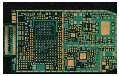
As can be seen from the computer board, there are three ways to install components. A plug-in installation process for transmission, in which electronic components are inserted into the through holes of the printed circuit board. In this way, it is easy to see that the through holes of double-sided printed circuit boards are as follows: one is a simple component insertion hole; the other is a component insertion and double-sided interconnection through hole; the third is a simple double-sided conduction Through holes; the fourth is the substrate mounting and positioning holes. The other two mounting methods are surface mounting and direct chip mounting. In fact, the direct chip mounting technology can be considered as a branch of surface mounting technology. It is to directly stick the chip on the PCB circuit board, and then use wire bonding or tape carrier method, flip chip method, beam lead method and other packaging technologies to interconnect to the PCB. Circuit board. The welding surface is on the component surface.