1. Annular Ring
Refers to the copper ring that is flatly attached to the PCB surface around the wall of the through hole. The hole ring on the inner plate is often connected to the outer ground by a cross bridge, and is more often regarded as the end of the line or the station. On the outer layer board, it can be used as a soldering pad for component pin soldering, in addition to being used as a circuit crossing station. There are Pad (with circle), Land (independent point) and so on that are synonymous with this word.
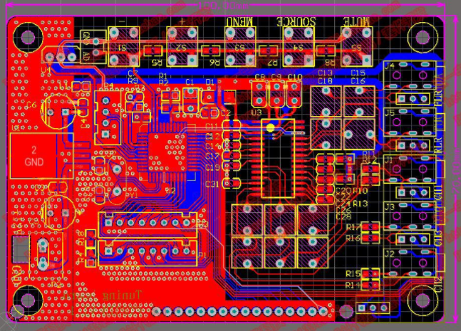
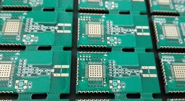
Professional terms commonly used in PCB circuit board design
2. Artwork film
In the circuit board industry, this word often refers to black and white negatives. As for the brown "Diazo Film" (Diazo Film), it is also named after Phototool. The negatives used in PCB can be divided into "original negatives" Master Artwork and re-photographed "working negatives" Working Artwork, etc.
3. Basic Grid
Refers to the vertical and horizontal grid where the conductor layout and positioning of the circuit board are designed. In the early days, the grid spacing was 100 mil. At present, due to the prevalence of fine lines and dense lines, the basic grid spacing has been reduced to 50 mils.
4. Blind Via Hole
Refers to the complex multi-layer board, because part of the vias only need a certain layer of interconnection, so they are deliberately incompletely drilled. If one of the holes is connected to the ring of the outer board, it is like a cup The special hole in the dead end is called "Blind Hole".

5. Block Diagram circuit system block diagram
The assembly board and the various components required are framed in square or rectangular empty boxes on the design drawing, and various electrical symbols are used to communicate the relationship between the frames one by one to form a systematic structure picture.
6. Bomb Sight bullet mark
Originally refers to the aiming screen where bombers dropped bombs. During the production of the negatives of the PCB, for the purpose of alignment, the upper and lower two-layer alignment targets are also set up at each corner. The more accurate official name should be called Photographers' Target.
7. Break-away panel can be disconnected
Refers to many small circuit boards. For the convenience of plug-in, component placement, soldering and other operations on the downstream assembly line, in the PCB manufacturing process, they are specially combined on a large board for various processing. When the work is completed, the method of jumping blades is used to perform a local cutting shape (Routing) disconnection between the independent small plates, but several "Tie Bar or Break-away Tabs" with sufficient strength are retained, and they are connected. Drill a few more small holes between the sheet and the edge of the board; or cut V-shaped notches up and down to facilitate the separation of the boards after the assembly process is completed. This kind of small board joint assembly method will be more and more in the future, IC card is an example.
8. Buried Via Hole
Refers to the local vias of the multilayer board. When they are buried between the inner layers of the multilayer board, they become "internal vias" and are not "connected" with the outer board, which are called buried vias or buried vias for short.
9. Bus Bar
Refers to the cathode or anode rod itself on the electroplating tank, or the cable to which it is connected. In the circuit board "in process", the outer edge of the gold finger is close to the edge of the board, the original connecting wire (which must be covered during the gold plating operation), and a small narrow piece (all for saving gold (It is necessary to reduce the area as much as possible) to connect with each finger. This kind of conductive connection is also called Bus Bar. The small piece where each individual finger is connected to the Bus Bar is called Shooting Bar. When the PCB board is finished cutting the shape, both will be cut off at the same time.
10. CAD computer-aided design
Computer Aided Design uses special software and hardware to digitally lay out the circuit board, and uses an optical plotter to convert the digital data into original film. This kind of CAD is far more accurate and convenient for the pre-manufacturing engineering of the circuit board than the manual method.
11. Center-to-Center Spacing
Refers to the Nominal Distance (Nominal Distance) from the center to the center of any two conductors on the board. If the conductors arranged in a row have the same width and spacing (such as the arrangement of gold fingers), then this "center-to-center spacing" is also called pitch.
12. Clearance room, clearance, empty ring
Refers to the inner layer of the multilayer board, if the conductor surface is not connected with the hole wall of the through hole, the copper foil around the through hole can be etched away to form an empty ring, especially called "empty ring". In addition, the distance between the green paint printed on the outer board and each ring is also called Clearance. However, due to the gradual increase in the density of the current board surface, the original room for this green paint has also been forced to be almost empty.
13. Component Hole
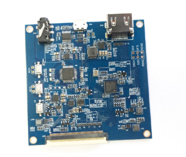
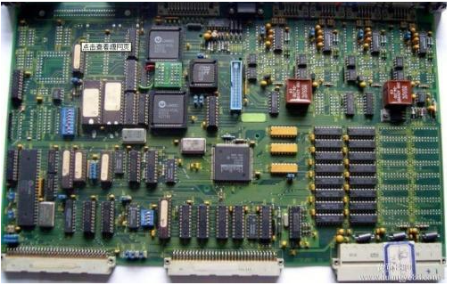
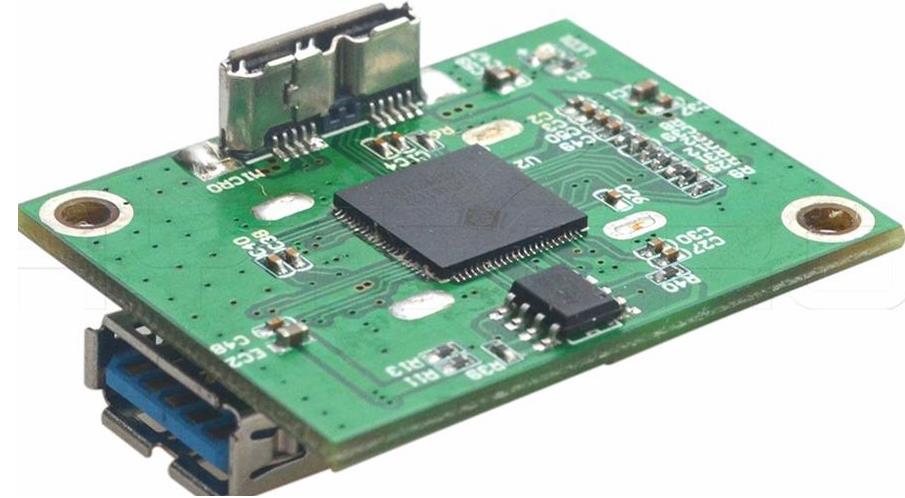
Refers to the through-holes for inserting parts on the board. The hole diameter of this pin hole is about 40 mils on average. Now that SMT has become popular, the number of large-aperture jacks has gradually decreased, and only a few gold pin holes of the connectors need to be plug-welded, and most of the remaining SMD parts have been surface-mounted.
In the early days when the circuit board was fully inserted with through-holes, the parts must be installed on the front of the board, so the front was also called the "component surface". The reverse side of the board is also called "Soldering Side" because only the tin wave of wave soldering passes through. At present, SMT boards have to attach parts on both sides, so there is no such thing as "component side" or "solder side", it can only be called front side or back side. Usually the name of the manufacturer of the electronic machine is printed on the front, and the UL code and production date of the circuit board manufacturer can be added on the back of the board.
15. Conductor Spacing conductor spacing
Refers to the span of a certain conductor on the circuit board surface from its edge to the edge of another nearest conductor, which is called the conductor spacing, or colloquially called the spacing. In addition, Conductor is a general term for various forms of metal conductors on circuit boards.
16. Contact Area contact resistance
On the circuit board, it refers to the contact point between the golden finger and the connector, and the resistance that appears when the current passes. In order to reduce the generation of oxides on the metal surface, usually the positive gold finger part and the female clip of the connector need to be plated with metal to prevent the occurrence of "load resistance". The plugs of other electrical products are squeezed into the socket, or there is contact resistance between the guide pin and its socket.
17. Corner Mark
On the negative of the circuit board, special marks are often left at the four corners as the actual boundary of the board. If the inner edge of these marks is connected, it is the boundary line of the contour of the finished board.
18. Counterboring fixed-depth reaming, counterboring
The circuit board can be locked and fixed in the machine with screws. For this matching non-through hole (NPTH), the hole must be a "reamed hole" that can accommodate the nut, so that the entire screw can sink into the board surface. In order to reduce the obstacles caused by appearance.