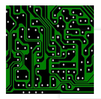
Beginners compare the following basic principles one by one while wiring while drawing on the PCB, and then use this rule to check again after the wiring is completed. Over time, there will be results. The ancients said: Foot, the ice is very hard. In the world, there are few geniuses after all, and only perseverance can achieve results.
[Experience] 1: The schematic diagram is based on the principle of convenient wiring and troubleshooting, reasonable use of the bus, and the use of real pin distribution.
[Experience] 2: Before generating the PCB, the package of all the unfamiliar devices should be made by hand, and the triode package should be made in advance.
[Experience] 3: Manual sketching should be carried out before wiring, and the general layout should be carried out under the principle of performance first.
[Experience] 4: The wiring should not be parallel to the axis of the component, carefully set the ground wire, and use full or grid copper plating appropriately.
[Experience] 5: The ground wire in the digital circuit should be networked, the signal clock wire should be used reasonably, and the pad should be appropriate.
[Experience] 6: Manual wiring should be based on the network or component wiring, and then the docking and arrangement between the blocks

[Experience] 7: When the layout is changed in an emergency, you must be calm. Generally, you only need to change individual components or one or two networks.
[Experience] 8: When making PCB, leave at least five solder holes, four corners and the center, in the blank space for aligning holes.
[Experience] 9: It is best to brush the tin before soldering. Put the components on the board first and fix them with tape before soldering.
[Experience] 10: The ADC circuit trace should be separated from the traces of other digital circuits or signal lines (especially the clock), and it is strictly forbidden to parallel and cross.
[Experience] 11: The oscillating crystal should be as short as possible and surrounded by a ground wire, but be careful not to increase the load capacitance due to the small spacing.
[Experience] 12: Single and double panels must have at least 50% metal layers, and multi-layer boards must have at least four metal layers to prevent local overheating and fire.
[Experience] 13: The signal wire should be as thick and short as possible. The signal wire and the input and output wires should be grounded, and the ground wire should be clamped between each module.
[Experience] 14: When the device pin is in contact with the ground wire, it is best not to use a large area of copper, but to use a grid. The entire board is also used for copper to prevent peeling.
[Experience] 15: If there is a large area of copper on the PCB board, several small openings should be made on the ground, but the hole should not be larger than 3.5mm, which is equivalent to a grid.
[Experience] 16: When using jumpers to avoid excessively long wiring, do not place the jumpers under large devices such as IC integrated blocks to facilitate plugging and unplugging.
[Experience] 17: The heat dissipation and ventilation of the device should be fully considered when layout and wiring, the heat source should be close to the edge of the board, and the distance between the test points should be designed.
[Experience] 18: The 20H rule and the 3W rule should be applied in the multi-layer anti-electromagnetic interference design to overcome the boundary radiation coupling and logic current magnetic flux interference.
[Experience] 19: It is best not to have dual signal lines in the same direction of current, and to control the minimum parallel length, such as using JOG wiring or sine and cosine wiring.
[Experience] 20: The interference caused by the change of the upper and lower edges of the signal in the low-frequency line is much greater than the interference caused by the frequency, so we must pay attention to the crosstalk problem.
[Experience] 21: The high-speed signal line should add proper termination matching, and it is best to keep its impedance unchanged during transmission, and widen the line width as much as possible.
[Experience] 22: Don't forget to add filtering and coupling capacitors between the power supply and ground of the integrated block to eliminate interference.
With the increasing density of modern integrated devices, the quality of the PCB layout directly affects the performance of the product, and even the key to the success or failure of the design. As an electronics expert said: There may be countless arrangements of ten kinds of devices. But if there is a little error, its performance may be a hundred times different! The importance and technicality of PCB layout can be seen.