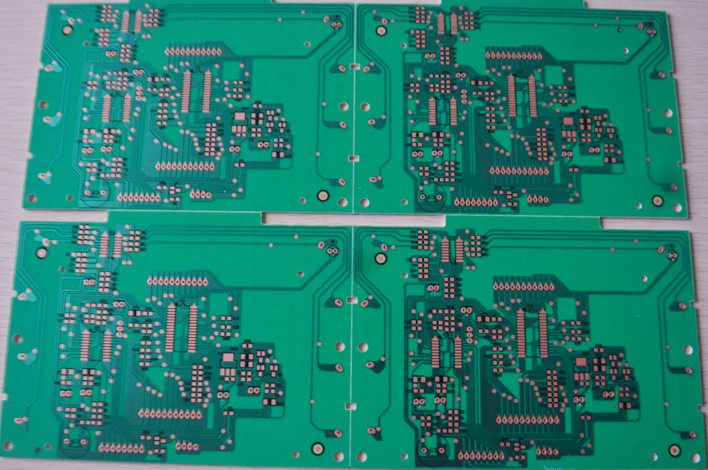
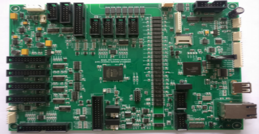
Good power supply circuit design needs good PCB layout and routing design to carry, the quality of PCB design is directly related to the performance of the circuit. In product switch caused by too much due to the PCB design problems in the process of revision, such as filter circuit and power circuit to the unreasonable design in terms of distance and Angle of near field coupling noise is serious, cause many times to modify EMI filter can not effectively reduce the transmission noise parameters, the product will have to optimize layout and cause redesign. In the process of product development, if you can follow some rules and avoid some common mistakes, you can effectively ensure the performance of the product. Here are some important PCB layout and wiring suggestions.

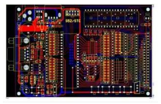
Overall layout of power supply
When the power PCB layout in advance, give priority to the power input - surge protection circuit slow up - EMI filter - a font layout, power supply module to avoid using u-shape layout, prevent leakage power within the high frequency magnetic field (high frequency transformer, power inductors, etc.) and filtering circuit coupled to the power input end, can lead to excess power transmission to low frequency test. If u-shaped layout is necessary due to other factors such as power supply structure, the power circuit and the filter circuit can be isolated by means of partition shielding, and the filter capacitor can also be reserved near the power connector.
EMI filter circuit layout
For EMI filter circuit, the differential mode capacitance before and after the common-mode inductor adopts Kelvin connection method, the copper skin under the common-mode inductor is holed out, and no other signals are taken. The Y capacitor on the right of the common-mode inductor must be placed close to the power module. Ensure that the Y capacitor is grounded with low impedance. If the Y capacitor is far from the screw, connect the Y capacitor to the screw with a copper skin of at least 250mil.
Three key circuits and voltage moving point layout
For the switching circuit and rectifier circuit in the power converter, the loop area must be controlled, because the larger the loop area, the greater the differential mode near field radiation, will interfere with the normal operation of the surrounding low voltage control signal and feedback signal. Voltage moving point is a very large DV/DT, the area of the moving point (the line connecting the switching device and the magnetic device) should be strictly controlled, and the width should be reduced as far as possible under the condition of meeting the same flow, otherwise the moving point will increase the lodging capacitance of the enclosure, resulting in increased radiation efficiency of the antenna and interference.
Layout of four magnetic components
For high-frequency transformers and inductors, the copper skin below it should be hollowed out, and the signal network should not go deep into the bottom, because the transformer and inductor itself is a high-frequency magnetic field source, which is easy to coupling noise to the network below.
Control circuit layout
Power circuits should be arranged separately from control circuits, because power circuits are generally high-voltage, high-current, high-frequency circuits, and their near-field interference is serious. And the control circuit is generally low voltage signal, its anti-interference ability is weak, so two separate layout. Moreover, the power and control ground should be separately wired, single point grounding, to prevent the power circuit and control circuit from common ground impedance coupling.
Drive circuit layout
The distance between the drive circuit and the switch tube should be short, and since the drive signal is also a large DI/DT interference source, the loop area of the drive signal line and ground wire should be controlled to.
Seven original side capacitor layout
The filter capacitor between the static point of the primary side and the static point of the secondary side should be placed close to the transformer and the switch tube, so as to reduce the common mode loop area of the primary side moving point - transformer primary stage anchoring capacitance - secondary side static point - primary side static point, provide low impedance backflow path for common mode noise, and reduce the noise current flowing to the LISN.
Eight epilogue
The above are some common rules for PCB layout and routing of power supply. It is more convenient for us to understand and memorize from the perspective of each circuit module. Through the study of this article, I believe that you have a deeper understanding of power EMI.