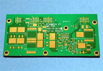
When PCB proofing plug-in component pads, the size of the pads should be appropriate. If the pad is too large, the spreading area of the solder will be larger, and the solder joint formed will not be full, while the surface tension of the copper foil of the smaller pad is too small, and the solder joint formed is a non-wetting solder joint. The cooperation gap between the aperture and the component line is too large, and it is easy to solder. When the aperture is 0.05~0.2mm wider than the lead wire and 2~2.5 times the diameter of the pad, it is an ideal condition for welding.
The PCB proofing in accordance with the requirements of the pad is to achieve a small diameter, which is at least 0.5mm larger than the large diameter of the small hole flange of the welding terminal. Test pads must be provided for all nodes in accordance with ANSI/IPC2221 requirements. A node is an electrical connection point between two or more components. A test pad requires a signal name (node signal name), the x-y coordinate axis related to the reference point of the printed circuit board, and the coordinate position of the test pad (clarify on which side of the printed circuit board the test pad is located).

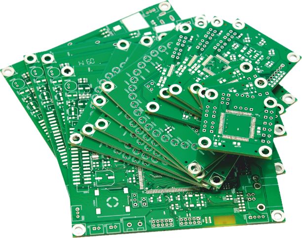
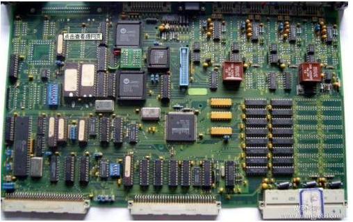
Considerations of PCB Proofing for the Size of the Pad Aperture
The aspect ratio of the plated through hole has an important influence on the ability of the PCB proofing manufacturer to perform useful plating in the plated through hole, and it is also important in ensuring the reliability of the PTH/PTV structure. When the size of the hole is less than 1/4 of the thickness of the basic circuit board, the tolerance should be increased by 0.05mm. When the hole diameter is 0.35mm or less and the aspect ratio is 4:1 or greater, the PCB proofing manufacturer should use appropriate methods to cover or block the plated through holes to prevent solder from entering. Generally speaking, the ratio of the thickness of the printed circuit board to the pitch of the plated through holes should be less than 5:1. It is required to provide information on the fixed equipment for smt, and it also needs the warming technology of the printed circuit board assembly layout to promote the development in the circuit with the help of "fixed equipment for circuit testing" or generally called "fixed equipment for nail bed". Testability.
In order to achieve this intent, it is necessary to:
1. Avoid plated through-holes-probing at both ends of the printed circuit board. Put the test top through hole on the non-component/soldering surface of the printed circuit board. This method allows the use of reliable and cheaper equipment. The number of different hole sizes should be kept low.
2. The diameter of the test pad dedicated to prospecting should not be less than 0.9mm.
3. Don't rely on the edge of the connector pointer for pad testing. The test probe can easily damage the gold-plated pointer.
4. The space around the test pad should be greater than 0.6mm and less than 5mm. If the height of the component is greater than 6.7mm, the test pad should be placed 5mm away from the component.
5. Do not place any components or test pads within 3mm from the edge of the printed circuit board.
6. The test pad should be placed in the center of a 2.5mm hole in a grid. If possible, promise to use standard probes and a more reliable fixture.
The above is all the considerations on the details of PCB proofing, all for product quality