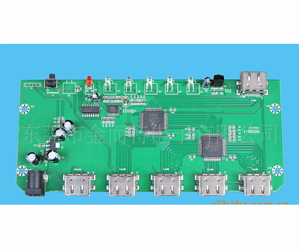
Today's electronic products can be said to be used around us all the time, and the PCB circuit boards used in various electronic products have different PCB colors and shapes, sizes and levels, and materials in different industries. Therefore, it is necessary to understand the information in the design of the PCB circuit board, otherwise it is easy to show misunderstandings.
1. The definition of the processing level is not clear: the single-sided board is designed in the TOP layer. If the positive and negative aspects are not clarified, it may be difficult to solder the board with components.

2. The distance between the large area copper foil and the outer frame is too close: the distance between the large area copper foil and the outer frame should be at least 0.2mm, because when milling the shape of the copper foil, it is easy to cause the copper foil to warp and cause resistance. Flux drop problem.
3. Draw pads with filler blocks: Draw pads with filler blocks can be checked by DRC when designing the PCB circuit board, but the processing is not good, so similar pads cannot directly generate solder mask data. When applying solder resist, The area of the filler block will be covered by the solder resist, causing difficulty in soldering the device.
4. The electrical ground layer is also a flower pad and a connection: because it is designed as a flower pad power supply, the ground layer is opposite to the image on the actual printed board. All connections are isolated lines. Draw several groups of power supplies or several grounds. Care should be taken when isolating the line, not leaving a gap, short-circuiting the two sets of power supplies, and not forming a blockade of the connection area.
Fifth, the characters are randomly placed: The SMD soldering pad of the character cover pad brings inconvenience to the on-off test of the printed circuit board and the soldering of the components. The character design is too small, it is difficult to form a screen printing, too large will make the characters stacked on top of each other, it is difficult to distinguish.
6. The pad of the surface mount device is too short: This is for the continuity test. For the surface mount device that is too dense, the distance between the two pins is quite small, and the pad is also quite thin. The device test needle must be interlaced up and down. The position, such as the design of the pad is too short, will not affect the device device, but will make the test pin not staggered.
7. Single-sided pad aperture setting: Single-sided pads are generally not drilled. If the drilling needs to be marked, the aperture should be designed to be zero. If a numerical value is designed so that when the drilling data is generated, the hole coordinates are displayed at this position, which presents a problem. Single-sided pads such as drilling should be specially marked.
8. Pad stacking: The drilling process in the PCB circuit board will cause the drill bit to be broken due to repeated drilling in one place and cause hole damage. Two holes in the multi-layer board are stacked, and the negative film is drawn as an isolation disk, forming a scrap.