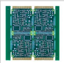
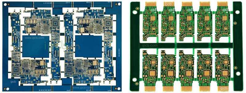
There are many industry terms for PCB design and manufacturing. As practitioners in the circuit board industry, they must be able to understand and apply these industry terms. This will not only better communicate with customers, but also reflect your professionalism. The following professional PCB design companies, circuit board manufacturers, PCBA processing manufacturers Shenzhen Honglijie Electronics will introduce the industry terminology of PCB design and manufacturing.
PCB design and manufacturing company
PCB design and manufacturing term 1: Impedance Bar (Test Coupon)
Test Coupon is used to use TDR (Time Domain Reflectometer) to measure whether the characteristic impedance of the produced PCB meets the design requirements. Generally, the impedance to be controlled includes single-ended and differential pairs, so test coupon The line width and line spacing (when there is a differential pair) on the trace should be the same as the line to be controlled, and the most important thing is the location of the grounding point during measurement. In order to reduce the inductance value of the ground lead, the grounding place of the TDR probe is usually very close to the signal measuring point (probe tip), so the distance and method between the measuring signal point and the ground point on the test coupon should be Meet the specifications of the probe used.

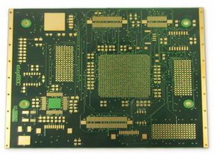
PCB design and manufacturing term 2: gold finger
The gold finger (or Edge Connector) is designed for the purpose of pressing and contacting the connection between the connector shrapnel and conducting the interconnection. Gold was chosen because of its superior conductivity and oxidation resistance. The row of golden things in your computer's memory stick or graphics card version is the golden finger.
Golden finger
The question is, is the gold on the gold finger gold? The hardness of pure gold is not enough, and the gold fingers have to deal with the frequent insertion and extraction actions. Therefore, compared with the "soft gold" of pure gold, the gold fingers are generally electroplated "hard gold", where the hard gold is electroplated alloy (that is, Au And other metal alloys), so the hardness will be harder.
PCB design and manufacturing term 4: hard gold, soft gold
Hard gold: Hard Gold; soft gold: soft Gold
Electroplating soft gold is to deposit nickel and gold on the circuit board by electroplating, and its thickness control is more flexible. Generally, it is used for aluminum wire on COB (Chip On Board), or the contact surface of mobile phone keys, while gold fingers or other adapter cards, and most of the electroplated gold used for memory is hard gold, because it must be wear-resistant.
To understand the origin of hard gold and soft gold, it is best to first understand the process of electroplating gold. Leaving aside the previous pickling process, the purpose of electroplating is basically to electroplate "gold" on the copper skin of the circuit board, but if "gold" and "copper" are in direct contact, there will be a physical reaction of electron migration and diffusion (potential It is necessary to electroplate a layer of "nickel" as a barrier layer first, and then electroplate gold on top of the nickel, so what we generally call electroplated gold, its actual name should be called "electroplated nickel gold".
The difference between hard gold and soft gold is the composition of the last layer of gold that is plated on. When plating gold, you can choose to electroplate pure gold or alloy. Because the hardness of pure gold is relatively soft, it is also called "soft gold". ". Because "gold" can form a good alloy with "aluminum", COB will particularly require the thickness of this layer of pure gold when making aluminum wires.
In addition, if you choose to electroplated gold-nickel alloy or gold-cobalt alloy, because the alloy will be harder than pure gold, it is also called "hard gold".
PCB design and manufacturing term 5: Through hole: Plating Through Hole referred to as PTH
The copper foil lines between the conductive patterns in the different layers of the circuit board are conducted or connected by this kind of hole, but it is not possible to insert component leads or copper-plated holes of other reinforcing materials. The printed circuit board (PCB) is formed by stacking many layers of copper foil. The copper foil layers cannot communicate with each other because each layer of copper foil is covered with an insulating layer, so they need to rely on vias for signal linking, so there is a Chinese via Title.
The through hole is also the simplest kind of hole, because when making it, you only need to use a drill or a laser to directly drill the circuit board, and the cost is relatively cheap. On the contrary, some circuit layers do not need to connect these through holes, but the through holes are through the whole board, which will be wasted, especially for the design of high-density HDI boards, where the circuit board is very expensive. So although through holes are cheap, they sometimes use up more PCB space.
PCB design and manufacturing
PCB design and manufacturing term 6: blind hole: Blind Via Hole (BVH)
The outermost circuit of the PCB is connected to the adjacent inner layer with a plated hole. Because the opposite side cannot be seen, it is called a "blind hole". In order to increase the space utilization of the PCB circuit layer, the "blind via" process was developed.
Blind holes are located on the top and bottom surfaces of the circuit board and have a certain depth. They are used to connect the surface line with the underlying inner line. The depth of the hole generally has a specified ratio (aperture). This production method requires special attention. The drilling depth must be just right. If you don't pay attention, it will cause difficulties in electroplating in the hole. Therefore, few factories will adopt this production method. In fact, it is also possible to drill holes for the circuit layers that need to be connected in advance in the individual circuit layers, and then glue them together, but more precise positioning and alignment devices are required.
PCB design and manufacturing term 7: Buried Via Hole (BVH)
Buried vias are the connections between any circuit layers inside the printed circuit board (PCB), but they are not connected to the outer layer, that is, they do not have the meaning of via holes extending to the surface of the circuit board.
This manufacturing process cannot be achieved by drilling after the circuit board is bonded. It must be drilled at the time of individual circuit layers, first partially bonding the inner layer, then electroplating, and finally bonding all. Since the operation process is more laborious than the original vias and blind holes, the price is also the most expensive. This manufacturing process is usually only used for high-density circuit boards to increase the space utilization of other circuit layers.