Consider the choice of PCB parts packaging.
In the entire PCB principle drawing stage, the component packaging and pad patterns that need to be carried out in the PCB layout stage should be considered. The following are some suggestions that should be considered when selecting components based on a component package.
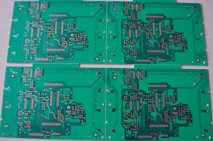
Remember that the package includes the electrical pad connections and mechanical dimensions (XY and Z) of the component, that is, the shape of the component and the pins that connect to the PCB. When selecting components, any installation or packaging restrictions that may exist on the top and bottom layers of the final PCB should be considered. Some components (such as polarized capacitors) may have a high degree of clearance restrictions that need to be considered in the component selection process. At the beginning of the design, you can first draw a basic circuit board frame, and then place some planned large or key components (such as connectors). In this way, you can intuitively and quickly see the virtual perspective view of the circuit board (without wires), and give a relatively accurate relative positioning and height of the circuit board and components. This will help ensure that after the PCB is assembled, the components can be properly placed in the outer packaging (plastic chassis frame), etc. Dial the 3D preview mode from the Tools menu to browse the entire circuit board.
The land pattern shows the actual land or perforation shape of the soldering equipment on the PCB. The copper pattern on the PCB also contains some basic shape information. The size of the disc pattern needs to ensure correct welding and the correct mechanical and thermal integrity of the connected parts. When designing the PCB layout, how to manufacture or manually solder the circuit board, should consider how to solder.

Reflow soldering (soldering is melted in a controlled high-temperature furnace) can handle a wide range of surface bonding devices (SMD). Wave soldering is usually used to solder the opposite side of the circuit board to fix the through-hole device, but it can also handle some surface sticker components placed on the back of the PCB. Normally, when using this technology, the bottom surface bonding device must be arranged in a specific direction, and the pad may need to be modified to accommodate this welding mode.
(3) The selection of components can be changed during the entire design process. In the early stages of the design process, determining which devices should use plated through holes (PTH) and which should use surface sticker technology (SMT) will help the overall planning of the PCB. The factors that need to be considered are the cost, availability, area density and power consumption of the equipment. From a manufacturing perspective, surface devices are generally cheaper than through-hole devices and are generally easier to use. For small and medium-sized prototype projects, it is best to choose large-scale surface equipment or through-hole devices, which not only facilitates manual soldering, but also facilitates better connection of pads and signals.
4. If there is no ready-made packaging in the database, custom packaging is usually created in the tool.
2. Use good grounding methods..
Ensure that the design has sufficient side capacitance and ground plane.. When using an integrated circuit, make sure to use a suitable decoupling capacitor near the ground near the power terminal. The appropriate capacity of the capacitor depends on the specific capacitor technology and operating frequency. When the bypass capacitor is set between the power and ground pins and is close to the correct IC pin, the electromagnetic compatibility and susceptibility of the circuit can be optimized.
Allocate virtual component packages.
Print a list of materials (BOM) to check the virtual components. Virtual components without related packaging will not be sent to the layout stage. Create a material list and check all the virtual components in the design. The only items should be power and ground signals, because they are considered virtual components and can only be handled in the context of the schematic, and will not be transmitted to the layout design. Unless for simulation purposes, the components shown in the virtual section should be replaced by packaging components.
4 Make sure you have complete bill of materials data.
Check if there is sufficient data in the list. After creating the bill of materials report, you should carefully check all PCB components for incomplete equipment supplier or manufacturer information.
Sort 5 according to the component label.
To help the order and review of the bill of materials, make sure that the component labels are numbered consecutively.
Check the extra gate circuit.
In general, all additional gate inputs should have signal connections to avoid hanging on the input end. Make sure you check all extra or missed gate circuits and all wireless inputs are fully connected. In some cases, if the input terminal is in a suspended state, the entire PCB system cannot work correctly. Take the double operation that is often used in the design. If the IC component is transported in both directions, it is recommended to use only one of the transmissions or the other transmission or not to use the transport input terminal to ground. And arrange a suitable unity gain (or other benefits) feedback network to ensure that the entire component can work normally.
In some cases, the suspension pin IC may not work properly. Generally, only when the IC device or other gates in the same device are in a saturated state, can the IC work to meet the index requirements. Simulation usually cannot capture this situation, because the simulation model usually does not connect multiple parts of the IC to build the model suspension connection effect.