In the entire PCB schematic drawing stage, the component packaging and land pattern decisions that need to be made in the layout stage should be considered. Some suggestions to consider when selecting components based on component packaging are given below.
Remember, the package includes the electrical pad connections and mechanical dimensions (X, Y, and Z) of the component, that is, the shape of the component body and the pins that connect to the PCB. When selecting components, you need to consider any mounting or packaging restrictions that may exist on the top and bottom layers of the final PCB. Some components (such as polar capacitors) may have high headroom restrictions, which need to be considered in the component selection process.

At the beginning of the design, you can first draw a basic circuit board frame shape, and then place some large or position-critical components (such as connectors) that you plan to use. In this way, the virtual perspective view of the circuit board (without wiring) can be seen intuitively and quickly, and the relative positioning and component height of the circuit board and components can be given relatively accurate. This will help ensure that after the PCB is assembled, the components can be properly placed in the outer packaging (plastic products, chassis, machine frame, etc.), and the whole circuit board can be viewed by calling the 3D preview mode from the tool menu.
The land pattern shows the actual land or via shape of the soldered device on the PCB. These copper patterns on the PCB also contain some basic shape information. The size of the land pattern needs to be correct to ensure correct soldering and the correct mechanical and thermal integrity of the connected components.
When designing the PCB layout, you need to consider how the circuit board will be manufactured, or how the pads will be soldered if it is manually soldered. Reflow soldering (the flux is melted in a controlled high temperature furnace) can handle a wide range of surface mount devices (SMD). Wave soldering is generally used to solder the reverse side of the circuit board to fix through-hole devices, but it can also handle some surface mount components placed on the back of the PCB. Generally, when using this technology, the bottom surface mount devices must be arranged in a specific direction, and in order to adapt to this soldering method, the pads may need to be modified.
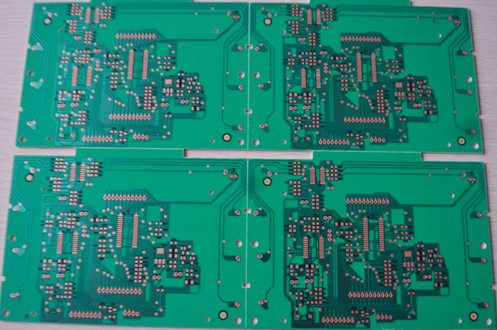
The selection of components can be changed throughout the design process. Determining which devices should use plated through holes (PTH) and which should use surface mount technology (SMT) early in the design process will help the overall planning of the PCB. Factors that need to be considered include device cost, availability, device area density, power consumption, and so on. From a manufacturing perspective, surface mount devices are generally cheaper than through-hole devices and generally have higher availability. For small and medium-scale prototype projects, it is best to choose larger surface mount devices or through-hole devices, which not only facilitate manual soldering, but also facilitate better connection of pads and signals during error checking and debugging.
If there is no ready-made package in the database, a custom package is usually created in the tool.