The following describes two basic design methods for reducing SSO based on the SSO generation mechanism for printed circuit boards equipped with FPGAs.
1. Design method to reduce inductive coupling
The simulation results show that the inductive coupling on the chip package/PCB interface is the culprit leading to high-frequency spikes in the SSO waveform. A signal loop with a size of t*d is composed of a signal via and the nearest ground via. The size of this loop indicates the strength of inductive coupling. The larger the area of the I/O interference loop, the easier it is for the generated magnetic field to invade the adjacent interfered loop. The larger the area of the interfered I/O signal loop, the more susceptible to interference from other I/O loops. Therefore, to reduce the crosstalk and the parameter t, a thinner PCB should be used in the design, and the key I/O on the PCB should be led out from a shallower signal layer. At the same time, designers can reduce crosstalk by shortening the distance between I/O vias and ground vias. The designer specially connects a pair of I/O pads to the ground plane and the VCCIO plane to reduce the signal loop area of the interfering pins and the interfered pins.

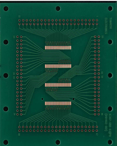
To evaluate the effectiveness of this method, two measurements were made on FPGA I/O Bank1 and Bank2. All I/O ports in these two banks are configured as LVTTL 2.5-V interfaces with a current intensity of 12mA, and are terminated with a 10pF capacitor through a 50Ω stripline.
In Bank1, pin AF30 is the disturbed pin. In the FPGA design, the 6 pins of W24, W29, AC25, AC32, AE31 and AH31 are programmed to logic "0", and they are connected to the ground plane of the PCB through vias. The five pins U28, AA24, AA26, AE28 and AE30 are programmed to logic "1" and connected to the VCCIO plane of the PCB. The other 68 I/O ports undergo state changes at the same time at a frequency of 10MHz, so they are pins that cause interference. For comparison, the I/Os W24, W29, AC25, AC32, AE31, AH31, U28, AA24, AA26, AE28, and AE30 are not programmed to be ground or VCCIO pins in Bank2, but they are left unused. Other 68 Both I/Os are still switched on and off at the same time.
Experimental tests show that the ground bounce on AF30 in Bank 1 has been reduced by 17% compared to G30 in Bank 2, and the power sag has also been reduced by 13%. The simulation results also verify this improvement. Since the appearance of the programmable ground pin shortens the distance d between the interference loop and the interfered loop, the reduction in SSO is expected. However, since the signal loop area in the chip package cannot be reduced, the degree of improvement is also limited.
2. Reduce PDN impedance through reasonable design
The impedance between the VCCIO and ground pins at the interface on the PCB is the most important criterion for the PDN performance evaluation of an FPGA chip. This input impedance can be reduced by using an effective decoupling strategy and using a thinner power/ground plane pair. But the most effective method is to shorten the length of the power vias that connect the VCCIO solder balls to the VCCIO plane. Moreover, shortening the power via will also reduce the loop formed by it and the adjacent ground via, making this loop less susceptible to changes in the state of the interfering I/O loop. Therefore, the VCCIO plane should be arranged closer to the top layer of the PCB during design.
Summary of this article
In this paper, a comprehensive analysis of the simulation of synchronous switching noise on a PCB with FPGA is carried out. The analysis results show that the crosstalk on the package and PCB interface and the PDN impedance distribution on the package and PCB are two important causes of SSO.
Related models can be used to help PCB designers reduce SSO and achieve better PCB designs. The article also introduces several methods to reduce SSO. Among them, reasonable allocation of signal layers and full use of programmable ground/power pins can help reduce PCB-level inductive crosstalk, and arranging VCCIO in a shallower position in the PCB stack can also reduce PDN impedance.