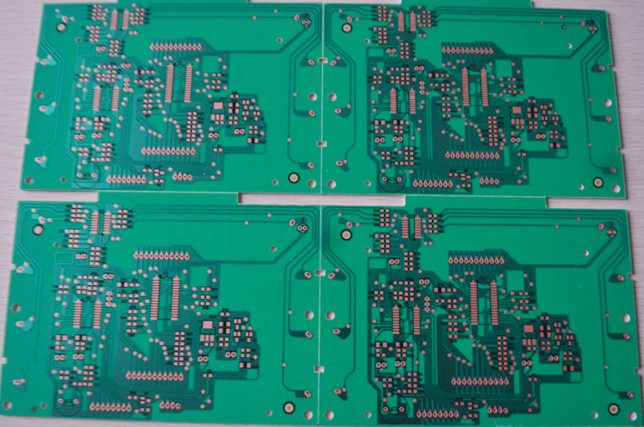
(1) Copper clad laminate in the PCB circuit board. Copper Clad Laminate (Copper Clad Laminate, full name Copper Clad Laminate, CCL in English) is made of wood pulp paper or fiberglass cloth as a reinforcing material, impregnated with resin, and covered with copper foil on one or both sides. Into a product. Copper clad laminate is the basic material of the electronics industry, mainly used for processing and manufacturing printed circuit boards. The current copper clad laminates in the electronic processing industry have also undergone a lot of updates. After many processes have been improved layer by layer, the volume has become smaller and smaller with the shrinking of electronic components, and the realized functions have become more and more complicated. .
(2) Copper foil wire. The substrate of the PCB itself is made of a copper clad laminate that is insulated and not flexible. The small circuit material that can be seen on the surface is copper foil. The copper foil was originally covered on the entire board, but part of it was etched away during the manufacturing process, and the remaining part became a network of small circuits. These lines are called wires or wiring, and are used to provide circuit connections for parts on the PCB circuit board. They are an important part of the PCB circuit board. The main attribute of the wire is the width, which depends on the size of the current carrying and the thickness of the copper foil. On printed circuit boards, copper foil has a certain influence on the electrical performance of electronic products. According to the manufacturing method, copper foil can be divided into two types: rolled copper foil and electrolytic copper foil. Rolled copper foil requires copper purity ≥99.9%, which is indicated by the letter W, and its copper foil has good elasticity and good solderability, and is suitable for high-performance PCB; electrolytic copper foil requires copper purity equal to 99.8%, which is indicated by the letter E, and it can be welded Slightly worse, suitable for ordinary PCB. Commonly used copper foil thickness is 9um, 12um, 18um. 35um, 70um, etc., among which 35um is used more. The thinner the copper foil, the worse the temperature resistance, and the leaching will make the copper foil penetrate; if the copper foil is too thick, it is easy to fall off. Therefore, at the beginning of the design of the schematic diagram of the circuit board, the electronic engineer has already considered that the size of each circuit and the realized function are set according to the rated amount of function and power.

(3) PCB pads. The pads are used for soldering components to achieve electrical connection and at the same time serve as fixing components. The basic properties of the pad include shape, layer, outer diameter and aperture. The pads of the double-layer board and the multi-layer board have been metallized on the hole wall. The metallization of the pad is an important link to achieve product stability and soldering stability. The quality of the pad determines the quality of the tin, while the quality of the printed circuit board is basically a problem of tin spots.
(4) Via hole. Vias are used to realize electrical connections between different working layers, and the inner walls of the vias are also metallized. Vias only provide electrical connections between different layers, and have nothing to do with the soldering and fixing of component pins. There are three types of vias. Passing through from the top layer to the bottom layer is called penetrating vias or through holes; vias that only connect the top or bottom layer with the middle layer are called blind holes, which reduces the depth of the hole; only realizes the middle layer connection without passing through The vias that penetrate the top or bottom layer are called buried holes, which can further reduce the depth of the hole. Although blind vias and buried vias are difficult to manufacture, they greatly improve the reliability of SMB manufacturing. Through the SMB light board test, it can be judged whether the line network is connected, and there is no need to worry about the fracture of the metallized hole due to unknowable external factors during the use of the product.
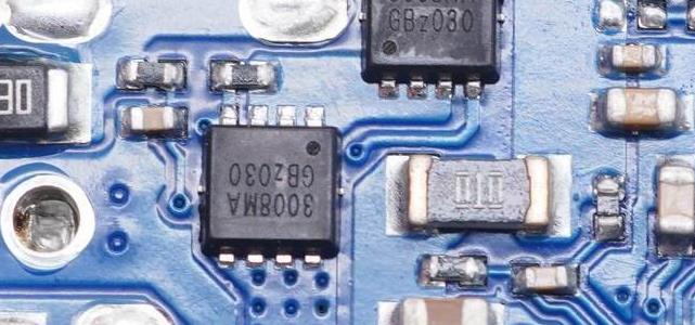
(5) Auxiliary testing equipment and image equipment. Among the components of the printed circuit board, testing equipment is indispensable. For example, PCB requires flying probe testing, and other processes require some auxiliary information, including graphics or text. The labels of various components and different graphic symbols reflect the shape and size of the contours of different components. In addition, the pin layout of the component together constitutes the package form of the component. The purpose of printing component graphic symbols is to display the information of the component on the PCB layout. It provides convenience for later assembly, debugging and maintenance.