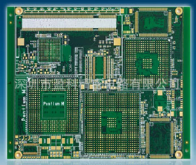
1) In the PCB design of low-power RF, standard FR4 materials are mainly used (good insulation properties, uniform material, dielectric constant ε=4, 10%). Mainly use 4-layer to 6-layer board. In the case of very sensitive costs, double-sided boards with a thickness of less than 1mm can be used. Ensure that the reverse side is a complete stratum. At the same time, the thickness of the double-sided board is above 1mm, making the stratum and signal layer The FR4 medium in between is thick. In order to make the impedance of the RF signal line reach 50 ohms, the width of the signal trace is often about 2mm, which makes it difficult to control the spatial distribution of the board. For a four-layer board, generally the top layer only uses RF signal lines, the second layer is a complete ground, and the third layer is a power supply. The bottom layer generally uses digital signal lines that control the state of the RF device (such as setting the clk, Data and LE signal lines.) It is better not to make the power supply of the third layer into a continuous plane, but to make the power lines of each RF device distributed in a star shape, and finally connect to a point. Do not cross the power traces of the third-layer RF devices with the digital lines on the bottom layer.
2) For a mixed-signal PCB, the RF part and the analog part should be far away from the digital part (this distance is usually above 2cm, at least 1cm), and the ground of the digital part should be separated from the RF part. It is strictly forbidden to use a switching power supply to directly supply power to the RF part. The main reason is that the ripple of the switching power supply modulates the signal of the RF part. This kind of modulation often severely damages the radio frequency signal, leading to fatal results. Under normal circumstances, the output of the switching power supply can be passed through a large choke coil, a π filter, and then a low-noise LDO (Micrel's MIC5207, MIC5265 series). For high-voltage, high-power RF circuits, You can consider using LM1085, LM1083, etc.) to get the power supply to the RF circuit.

3) In the RF PCB, each component should be arranged closely to ensure the shortest connection between each component. For the ADF4360-7 circuit, the distance between the VCO inductor on the pin-9 and pin-10 pins and the ADF4360 chip should be as short as possible to ensure that the distributed series inductance caused by the connection between the inductor and the chip is minimized. For the ground (GND) pins of each RF device on the board, including the pins connecting resistors, capacitors, inductances and ground (GND), holes and ground planes should be drilled as close as possible to the pins (second Layer) connected.
4) When choosing components to work in a high-frequency environment, use surface mount components as much as possible. This is because surface mount components are generally small in size and the component leads are very short. In this way, the influence of additional parameters caused by component pins and internal wiring of the component can be minimized. Especially for discrete resistors, capacitors, and inductance components, using a smaller package (0603\0402) is very helpful to improve the stability and consistency of the circuit;
5)In the PCB layout and design, active devices working in a high-frequency environment often have more than one power supply pin. At this time, you must pay attention to setting a separate power supply pin near each power supply pin (about 1mm). Even capacitance, the capacitance value is about 100nF. When the board space permits, it is recommended to use two decoupling capacitors for each pin, the capacitance values are 1nF and 100nF respectively. Generally, ceramic capacitors made of X5R or X7R are used. For the same RF active device, different power pins may power different functional parts in the device (chip), and each functional part in the chip may work at different frequencies. For example, the ADF4360 has three power pins, which supply power to the on-chip VCO, PFD, and digital parts. These three parts realize completely different functions, and the operating frequency is also different. Once the low-frequency noise of the digital part is transmitted to the VCO part through the power trace, the output frequency of the VCO may be modulated by this noise, causing spurs that are difficult to eliminate. In order to prevent this from happening, in addition to using separate decoupling capacitors, the power supply pins of each functional part of the active RF device must also be connected together through an inductive magnetic bead (about 10uH). This design is very beneficial to the improvement of the isolation performance of the active mixers LO-RF and LO-IF that include LO buffer amplification and RF buffer amplification.