PCB (Printed Circuit Board), the Chinese name is printed circuit board, also known as printed circuit board, printed circuit board, is an important electronic component, as the most versatile electronic component product, PCB has a strong vitality. After the reform and opening up for more than 20 years, due to the introduction of foreign advanced technology and equipment, single-panel, double-panel and multi-layer boards have achieved rapid development.
PCB (Printed Circuit Board), the Chinese name is printed circuit board, also known as printed circuit board, printed circuit board, is an important electronic component, as the most versatile electronic component product, PCB has a strong vitality. After the reform and opening up for more than 20 years, due to the introduction of foreign advanced technology and equipment, single-sided, double-sided and multi-layer boards have achieved rapid development. The domestic PCB industry has gradually developed from small to large, maintaining a high-speed growth of about 20% every year. From the perspective of output composition, the main products of China's PCB industry have shifted from single-sided and double-sided to multi-layer boards, and are increasing from 4-6 layers to 6-8 layers or more. As a new breakthrough in technology, PCB with its flexible design, stable and reliable electrical performance and superior economic performance has aroused many customers' curiosity about its design essentials.
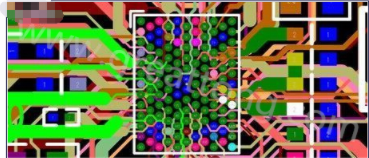
Multi-layer printed board refers to a printed board with more than two layers. It is composed of connecting wires on several layers of insulating substrates and pads for assembling and welding electronic components. The role of insulation. Therefore, the design of printed boards must be cautious and follow the necessary principles.
1. Necessary work for printed board design

Check the schematic diagram carefully: the design of any printed board is inseparable from the schematic diagram. The accuracy of the schematic diagram is the prerequisite basis for the correctness of the printed board. Therefore, before the design of the printed board, the signal integrity of the schematic must be carefully and repeatedly checked to ensure the correct connection between the devices.
Component selection: The selection of components is a very important link for the design of printed circuit boards. Devices with the same functions and parameters, and packaging methods may be different, and the packaging is different, and the solder holes (disks) of the devices on the printed board are different. Therefore, before embarking on the printed board design, we must determine the packaging form of each component.
Second, the basic requirements of multi-layer printed board design
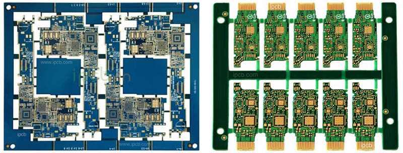
1. Determination of board shape, size and number of layers
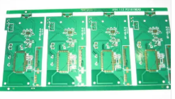
Any printed board has the problem of matching with other structural parts. Therefore, the shape and size of the printed board must be based on the structure of the product. However, from the perspective of the production process, it should be as simple as possible, generally a rectangle with a not too wide aspect ratio to facilitate assembly, improve production efficiency, and reduce labor costs.
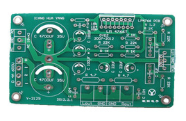
The number of layers must be determined according to the requirements of circuit performance, board size and circuit density. For multi-layer printed boards, four-layer and six-layer boards are the most widely used. Taking a four-layer board as an example, it has two conductor layers (component surface and soldering surface), a power layer and a ground layer.
The layers of the multilayer board should be symmetrical, and preferably the idol copper layer, that is, four, six, eight, etc. Because of the asymmetrical lamination, the board surface is prone to warping, especially for surface-mounted multilayer boards, which should be paid more attention.
2. Position and placement direction of components
The location and placement direction of the components should first be considered from the circuit principle to cater to the direction of the circuit. Whether the placement is reasonable or not will directly affect the performance of the printed board, especially the high-frequency analog circuit, which makes the location and placement requirements of the device more stringent.
3. Requirements for wire layout and wiring area
Under normal circumstances, multilayer printed board wiring is carried out according to circuit functions. When wiring on the outer layer, more wiring is required on the soldering surface and less wiring on the component surface, which is conducive to the maintenance and discharge of the printed board. Thin, dense wires and signal wires that are susceptible to interference are usually arranged in the inner layer. Large-area uranium foil should be more evenly distributed in the inner and outer layers, which will help reduce the warpage of the board and also obtain a more uniform coating on the surface during electroplating. In order to prevent the shape processing from damaging the printed guide wires and the interlayer short circuit caused by the mechanical processing, the distance between the conductive pattern of the inner and outer layer wiring area and the edge of the board should be greater than 50 mils.
4. Requirements for wire orientation and line width
Multilayer board wiring should separate the power layer, ground layer and signal layer to reduce interference between power, ground, and signals. The lines printed on two adjacent layers should be as perpendicular to each other as possible, or follow diagonal lines or curves, and not parallel lines, so as to reduce the coupling and interference between the substrate layers. And the wire should be short-circuited, especially for small signal circuits, the shorter the wire, the smaller the resistance, and the smaller the interference.
5. Drilling size and pad requirements
The size of the drilling holes of the components on the multilayer board is related to the size of the selected component pins. If the drilling is too small, it will affect the assembly and tinning of the device; if the drilling is too large, the solder joints are not full enough during welding. Generally speaking, the calculation method of component hole diameter and pad size is:
Aperture of component hole = component pin diameter (or diagonal) + (10-30mil)
Component pad diameter ≥ component hole straight length +18mil
As for the via hole diameter, it is mainly determined by the thickness of the finished board. For high-density multilayer boards, the board thickness should generally be controlled within the range of the hole diameter ≤ 5:1. The calculation method of the via pad is:
The diameter of the via pad (VISPAD) is ≥+12mil.
6. Requirements for power supply layer, stratum zone and flower hole:
For multilayer printed boards, there is at least one power layer and one ground layer. Since all voltages on the printed circuit board are connected to the same power layer, the power layer must be partitioned and isolated. The size of the partition line is generally 20-80mil line width. The voltage is super high and the partition line is thicker.
7. Requirements for safety clearance
The setting of the safety distance should meet the requirements of electrical safety. Generally speaking, the minimum spacing of the outer conductors shall not be less than 4mil, and the minimum spacing of the inner conductors shall not be less than 4mil. In the case that the wiring can be arranged, the spacing should be as large as possible to improve the yield during board manufacturing and reduce the hidden danger of failure of the finished board.
8. Requirement to improve the anti-interference ability of the whole board
In the design of multi-layer printed boards, attention must also be paid to the anti-interference ability of the entire board. The general methods are:
A. Add filter capacitors near the power and ground of each IC, the capacity is generally 473 or 104;
B. For sensitive signals on the printed board, the accompanying shielding wires should be added separately, and there should be as little wiring as possible near the signal source.
C. Choose a reasonable grounding point.
Third, multi-layer printed board outsourcing processing requirements
The processing of printed boards is generally outsourcing processing, so when providing drawings for outsourcing processing, Yi Cong must be accurate and clear as much as possible. Pay attention to the selection of materials, the order of laminating, the thickness of the board, the tolerance requirements, The processing technology, etc., must be clearly explained. When exporting GERBER from PCB, it is recommended to use RS274X format to export data, because it has the following advantages:
The CAM system can automatically enter data, and the whole process does not require manual participation, which can avoid a lot of troubles, while maintaining a lot of consistency and reducing the rate of business trips.
In addition to following the above design requirements, the design of the printed circuit board also needs to consider various factors such as the layout of external connections, the optimized layout of internal electronic components, the optimized layout of metal connections and through holes, electromagnetic protection, and heat dissipation. Among these factors, the PCB connector plays an extremely important pivotal role. Therefore, I would like to remind everyone: Although the design process is important, the choice of excellent connector products must not be ignored.