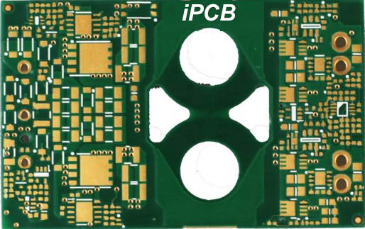
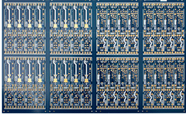
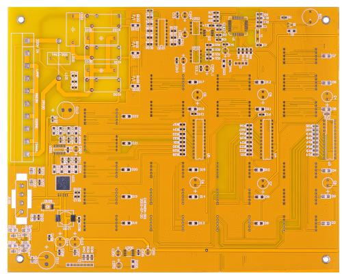
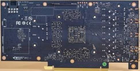
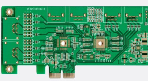
Products with a three-layer PCB
or more are called multilayer PCBs. The traditional double-sided board is a dense assembly of matching parts. It is impossible to place so many components and a large number of lines derived from it on a limited board surface, so there are multiple layers. The development of PCB boards.
The original four-layer PCB boards are mostly upgraded to six-layer PCB boards. Of course, high-level multilayer PCB boards are also increasing due to high-density assembly. This chapter will discuss the inner layer production and precautions of multilayer PCB boards.
Production process
According to different products, there are three kinds of processes
A.Print and Etch
Sending - Alignment hole - Copper surface treatment - Image transfer - Etching - Stripping
B. Post-etch Punch
Sending - copper surface treatment - image transfer - etching - peeling film - tool hole
C.Drilland Panel-plate
Sending - Drilling - Through Hole - Plating - Image Transfer - Etching - Stripping
Issue
Sending the material is to cut the substrate according to the BOM according to the working size planned by the pre-production design. It is a very simple step, but the following points must be paid attention to:
A. Cutting method-will affect the cutting size
B. Considerations of edging and rounding-affecting the image transfer yield process

C. The direction should be the same-that is, the warp direction is opposite to the warp direction, and the latitude direction is to the weft direction
D. Baking before the next process-consideration of dimensional stability
Copper surface treatment
In the printed circuit board manufacturing process, no matter which step, the effect of cleaning and roughening the copper surface is related to the success or failure of the next process, so it seems simple, but in fact there is quite a lot of knowledge.
A. The processes that require copper surface treatment are as follows
a. Dry film pressing
b. Before the inner layer oxidation treatment
c. After drilling
d. Before chemical copper
e. Before copper plating
f. Before the green paint
g. Before spraying tin (or other solder pad processing procedures)
h. Gold finger before nickel plating
This section discusses the best way to deal with processes such as a.c.f.g. (the rest are part of the process automation and do not need to be independent)
B. Treatment method
The current copper surface treatment methods can be divided into three types:
a.Brush
b. Sandblasting method (Pumice)
c. Chemical method (Microetch)
The following is an introduction to these three methods
Brushing
a. The effective length of the brush wheel must be used evenly, otherwise it is easy to cause uneven surface height of the brush wheel
b. The brush mark experiment must be done to determine the advantages of brush depth and uniformity
a. Low cost
b. The manufacturing process is simple, and the shortcomings of flexibility
a. Thin circuit boards are not easy to carry out
b. The base material is elongated, which is not suitable for the inner sheet
c. When the brush marks are deep, it is easy to cause D/F adhesion and infiltration
d. There is potential for residual glue
Sandblasting
The advantages of using fine stones of different materials (commonly known as pumice) as abrasive materials:
a. The surface roughness and uniformity are better than the brushing method
b. Better size stability
c. It can be used for thin plates and thin wires. Disadvantages:
a.Pumice is easy to stick to the surface
b. Machine maintenance is not easy
Chemical method (micro-etching method)
Image transfer
Printing method