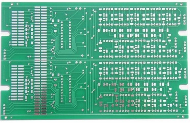
After designing the circuit structure and device location, PCB EMI control becomes extremely important for the overall design. How to avoid PCB electromagnetic interference in the switching power supply has become a topic of great concern to developers.
The component layout practice has proved that even if the PCB schematic design is correct and the printed circuit board is not properly designed, it will adversely affect the reliability of electronic equipment. For example, if the two thin parallel lines of the printed board are close together, the signal waveform will be delayed and reflected noise will be formed at the terminal of the transmission line. The performance drops, so when designing the printed circuit board, you should pay attention to adopting the correct method.
Each switching power supply has four current loops:
(1) AC circuit of power switch;
(2) Output rectifier AC circuit;
(3) Current loop of input signal source;
(4) Output load current loop.
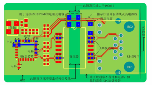
The input circuit charges the input capacitor through an approximate DC current, and the filter capacitor mainly serves as a broadband energy storage; similarly, the output filter capacitor is also used to store high-frequency energy from the output rectifier and eliminate the DC energy of the output load circuit. . Therefore, the terminals of the input and output filter capacitors are very important. The input and output current loops should only be connected to the power supply from the terminals of the filter capacitor respectively; if the connection between the input/output loop and the power switch/rectifier loop cannot be connected to the capacitor The terminal is directly connected, and the AC energy will be radiated into the environment by the input or output filter capacitor.

The AC circuit of the power switch and the AC circuit of the rectifier contain high-amplitude trapezoidal currents. The harmonic components of these currents are very high. The frequency is much greater than the fundamental frequency of the switch. The peak amplitude can be as high as 5 times the amplitude of the continuous input/output DC current. The transition time is usually About 50ns. These two loops are the most prone to electromagnetic interference, so these AC loops must be laid out before the other printed lines in the power supply. The three main components of each loop are filter capacitors, power switches or rectifiers, inductors or transformers. Place them next to each other and adjust the position of the components to make the current path between them as short as possible. The best way to establish a switching power supply layout is similar to its electrical design. The best design process is as follows:
Place the transformer
Design the power switch current loop
Design output rectifier current loop
Control circuit connected to AC power circuit
Design the input current source loop and input filter When designing the output load loop and output filter according to the functional unit of the circuit, when laying out all the components of the circuit, the following principles must be met:
(1) First, consider the PCB size. When the PCB size is too large, the printed lines will be long, the impedance will increase, the anti-noise ability will decrease, and the cost will increase; if the PCB size is too small, the heat dissipation will not be good, and adjacent lines will be easily disturbed. The best shape of the circuit board is rectangular, and the aspect ratio is 3:2 or 4:3. The components located on the edge of the circuit board are generally not less than 2mm away from the edge of the circuit board.
(2) When placing the device, consider the subsequent soldering, not too dense.
(3) Take the core component of each functional circuit as the center and lay out around it. The components should be uniformly, neatly and compactly arranged on the PCB, minimize and shorten the leads and connections between the components, and the decoupling capacitor should be as close as possible to the VCC of the device.
(4) For circuits operating at high frequencies, the distributed parameters between components must be considered. Generally, the circuit should be arranged in parallel as much as possible. In this way, it is not only beautiful, but also easy to install and weld, and easy to mass produce.
(5) Arrange the position of each functional circuit unit according to the circuit flow, so that the layout is convenient for signal circulation, and the signal is kept in the same direction as possible.
(6) The first principle of the layout is to ensure the wiring rate, pay attention to the connection of the flying wires when moving the device, and put the devices with the connection relationship together.
(7) Reduce the loop area as much as possible to suppress the radiation interference of the switching power supply