1, words before
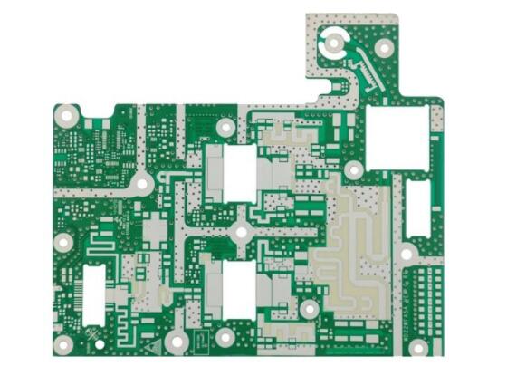
Integrated circuit packaging substrate can also be called IC packaging substrate (IC PCB), IC seal loading board, IC packaging substrate, is the carrier of integrated circuit chips, but also one of the key materials of high-density packaging, in the packaging of chip support, heat dissipation, protection, power distribution and electrical signal transmission and other functions. Organic packaging substrate has the advantages of low dielectric constant, low mass density, simple processing technology, high production efficiency and low cost, so it is the substrate type with the highest market share at present.
The organic packaging substrate is developed on the basis of the manufacturing principle and process of the traditional printed circuit board (PCB). Due to the smaller size and more complex electrical structure of the packaging substrate, it is much more difficult to manufacture than ordinary PCB. According to different physical properties and application fields, organic substrates can be divided into rigid organic packaging substrates and flexible organic packaging substrates.
The cost of organic packaging substrate occupies a high proportion in the chip packaging, which belongs to the low-end lead bonding substrate accounted for about 40%~50% of the total packaging cost, while the cost of high-end flip-chip substrate accounted for as high as 70%~80%. With the development of packaging technology, packaging substrate plays a more and more important role in promoting the progress of IC packaging industry. This report mainly focuses on the state of the organic packaging substrate industry research, and its technology and market development trend analysis.
2, State of domestic organic packaging substrate industry
2.1 . Domestic industry distribution
Domestic organic packaging substrate industry started late, and the breakthrough of packaging substrate industrialization was realized after 2009. At present, because the domestic chip design and packaging is still in the middle and low end, the lead frame packaging occupies a relatively high proportion, and the proportion of domestic packaging substrate packaging materials is far lower than the global market. In addition, the gap in key raw materials, equipment and technology, domestic enterprises in the level of technology, process capacity and market share is still lagging behind.
According to the statistics of China Electronic Circuit Industry Association, the output value of China's printed circuit board industry in 2019 was 227.499 billion yuan, of which the output value of packaging substrate was 7.492 billion yuan, up 18.59% year on year, accounting for 3.29% of the total output value. In 2019, the sales of packaging substrate of domestic enterprises exceeded 3 billion yuan, accounting for about 5% of the global market, and the market demand showed a high growth trend. At present, the mass production products of domestic enterprises are mainly low-end substrate products applied to lead bonding packaging, while the high performance multilayer substrate products applied to flip-chip packaging are still in the research and development stage, and there is a gap with the international advanced level. High-end organic substrate technology from the process, materials, equipment and so on are almost all monopolized by foreign enterprises, domestic enterprises are weak in technical force, lack of customer resources, high-end packaging substrate research and development investment is less.
Due to market and labor costs, international semiconductor manufacturers and packaging and test contract manufacturers have shifted their packaging capacity to China. The main foreign companies in the Chinese mainland market are three Taiwanese companies and one Austrian company: Taiwan UMTC (xin xing electronics), Kinsus (Kinsus), circuit board and South Asia, have IC package substrate factory in suzhou and kunshan, AT&S (Mr Winters) is equipped with IC package substrate project in chongqing, the foreign capital enterprise production accounts for about 60% of the domestic organic encapsulation base board market above, but the manufacture of high-end packaging substrate is not mass production in mainland China.
The domestic enterprises that take the lead in the packaging substrate industry mainly include: Shennan Circuit Co.,Ltd. (shennan Circuit), Anchelle Industry Co.,Ltd. (Anchelle), Zhuhai Yueya Packaging Substrate Technology Co.,Ltd. (Zhuhai Yueya), Xingsen Express Circuit Technology Co.,Ltd. (Xingsen Express), Shenzhen Danbond Technology Co.,Ltd. (Shenzhen Danbond), etc. Some PCB manufacturers are also paying attention to and entering the field of packaging substrate, respectively in Shenzhen, Wuxi, Zhuhai, Nantong and other places to set up factories or invest in new projects.
2.2 . Introduction of major domestic enterprises
Development of China's high-tech organic IC packaging and packaging substrate, has seized the attention of many, represented by shennan circuit, ansett substrate enterprises in high density organic packaging substrate continue to input in the technology development and industrialization projects, increase the independent intellectual property rights and national related standards, and achieved some breakthrough. Some technologies and products have reached the leading level in China and the advanced level in the world, breaking the monopoly of foreign giants, filling the gap in the domestic packaging substrate industry, and forming a certain market scale. Table 1 is the basic situation of the main domestic manufacturers of packaging substrate.
2.3 . Market analysis
The international well-known chip manufacturers and sealing testing enterprises have actively arranged and invested to expand production capacity in China, which has directly driven the rapid expansion of the scale of China's semiconductor packaging industry. The growing scale of China's chip manufacturing and the rapidly growing market for terminal electronics applications have also greatly boosted the growth of China's semiconductor packaging industry. With the support of national science and technology major projects, with long telegram technology, ansett, rich micro electricity, huatian technology and other advanced packaging enterprises of domestic packaging industry is also developing packaging substrate based packaging materials, laminated, system-level integration chip packaging technology and 3 d packaging technology, which will further drive the rapid development of domestic testing industry chain. Therefore, China's high-end packaging substrate market potential is huge, organic packaging substrate localization process is particularly important.
2.4 . Technology roadmap
With the rapid development of packaging technology, the characteristics of semiconductor packaging devices such as miniaturization, miniaturization, multi-function, high frequency, high speed, high performance and low cost are more and more transferred to the packaging substrate. In order to meet the needs of advanced packaging development, organic packaging substrate should be improved and optimized in terms of increasing wiring density, reducing thickness, and improving mechanical/heat transfer/electrical performance.
It is generally considered that the technical index of flip chip substrate can represent the technological level of organic packaging substrate. In the field of rigid packaging substrate, Nanya Technology's technology roadmap for flip-chip substrate with ABF lamination structure is shown in Table 2. The number of substrate layers will be more than 22, the area of a single substrate will be further increased to 100 mm*100 mm to increase the I/O number, and the core thickness will be reduced to 150 mm to reduce the packaging height. The aperture of the through hole is reduced to 80 mm, the aperture of the blind hole is reduced to 55 mm, and the blind hole is stacked to 6 layers. The dry film process makes the line width/line distance up to 8 mm /8 mm, the thickness of the solder resistance layer down to 10 mm, and the pitch of the convex point down to 90 mm. The above technical indicators are to achieve high performance, high density, thin packaging products in the direction of development.
The technology roadmap of domestic substrate suppliers for flip-chip packaging substrate is shown in Table 3. It can be seen that although domestic enterprises still have a gap with the advanced level, they have already had the substrate processing technology ability, and are approaching the leading technology.
In the field of flexible packaging substrate, The process roadmap of The semi-addition method is shown in Table 4, and the products with the minimum line width/line spacing of 8 μm/8 μm and the minimum aperture of 10 μm are prepared. Compared with the technical indicators of similar products at home and abroad, the indicators reach the domestic leading level and the international advanced level.
2.5 . Annual development of leading enterprises
In recent years, benefiting from the strong support of national policies and the huge domestic market demand, the domestic semiconductor industry has entered the fast track of development. As a key material in the semiconductor packaging industry chain, the domestic alternative demand for packaging substrate is strong. In 2019, some domestic substrate enterprises have achieved rapid development.
As a leading enterprise In the field of rigid packaging substrate In China, Abie Circuit focuses on the field of electronic interconnection and is committed to "building a world-class integrator of electronic circuit technology and solutions". It has three businesses of printed circuit board, packaging substrate and electronic assembly and connection, forming a unique "3-in-one" business layout In the industry. At present has formed with independent intellectual property rights package substrate production technology and process, to adapt to the operating system in the field of integrated circuit is established, and become a violet light show sharp, ase, rely on science and technology, silicon products, song, acoustics, sound, long telegram technology, huatian technology such as the world's leading IC design, testing and device manufacturers long-term cooperation partner. We have a leading competitive advantage in some market segments. For example, the company in silicon microphones microelectromechanical packaging substrate field, technology
Leading in the world, the products are widely used in smartphones such as Apple and Samsung, with a global market share of more than 30%. Rf module packaging substrate is widely used in 3G, 4G mobile phone RF module packaging; High-end memory chip packaging substrates for embedded memory chips have been mass produced. In terms of processor chip packaging substrates, flip - over packaging (FC-CSP) substrates are now available for mass production. The company actively expanded production of packaging substrate, leading the wave of replacing imported products with domestic substrate. Wuxi substrate factory for storage packaging substrate products started trial production in June 2019, and is now in the stage of capacity climbing. In 2019, the operating revenue of packaging substrate business reached 1.164 billion yuan, up 22.94% year on year, accounting for 11.06% of the company's total operating revenue. The r&d investment of the company reached 537 million yuan, with a year-on-year growth of 54.77%, accounting for 5.10% of the total revenue of the company. The company mainly invests in the next generation communication printed circuit board and storage packaging substrate, and mainly targets at key areas such as high density, high integration, high speed and high frequency, high heat dissipation and miniaturization. The company has been authorized 455 patents, including 357 invention patents and 22 international PCT patents. The number of patents authorized ranks among the top in the industry.

As the earliest manufacturer of flexible circuit board and flexible packaging substrate in China, IPCB is committed to building a one-stop service system for the design and manufacturing of "flexible printed circuit board -- flexible packaging substrate -- module assembly". Our business covers the manufacturing of high density flexible printed circuit board (PCB), soft and hard combined board (PCB), packaging substrate and electronic surface mount module assembly. We have set up two production bases in Guangzhou and Suzhou. Our customers cover communication, computer, financial IC card, automotive electronics, consumer electronics, medical equipment and aerospace and other fields. Our customers are mainly large domestic and foreign electronic information enterprises, and we have formed close cooperative relations with many domestic and foreign mainstream electronic information enterprises. The products are widely used in the main products of Finisar, Huawei, Goer Acoustics, Sainty Optics, Qiuti Technology, Ophioponics, Freescale, TCL, Samsung, Avago, TriQuint and other companies, and have been widely recognized by customers. In addition, through equity cooperation, Angelica products have successfully entered the industrial chain of Apple and Tesla, bringing new development opportunities. At the same time, in order to welcome the development of the new generation of 5G industry, The COMPANY has successfully developed the LCP flexible packaging substrate for 5G, which provides the necessary material guarantee for the commercial use of 5G industry and fills the gap in China. In 2019, the strong growth of flexible packaging substrate business, sales reached 390 million YUAN, a year-on-year increase of 39.28%, further consolidating its leading advantage in the flexible packaging substrate industry.
Ipcb entered the packaging substrate industry in 2012, becoming the first manufacturer to enter this field in China. After several years of accumulation, the company has gradually mastered the key technologies in the packaging substrate process, and has continuously achieved breakthroughs in customers, technology and process capabilities. Core indicators such as the packaging substrate yield and capacity utilization have been improved. In 2019, the sales revenue of packaging substrate business reached 297 million yuan, with a year-on-year growth of 26.04%, accounting for 7.82% of the company's total operating revenue. In 2019, the company invested 198 million yuan in RESEARCH and development, accounting for 5.2% of the company's total revenue. The company mainly conducted systematic research and attack in a number of technical fields, such as passive intermodulation control technology of 5G antenna, high frequency and high speed signal integrity control technology, analysis and prediction of big data of growth and contraction. Among them, the key development of embedded line (ETS) packaging substrate, overcome the production of 35 mm thick copper MSAP process line, buried line process development, high heat dissipation buried line production in the way of buried line and other key technologies, break through the foreign technology monopoly, realize the development and industrialization of thick copper high heat dissipation buried line packaging substrate for intelligent equipment. Help the rapid development of China's integrated circuit packaging substrate industry. The company has granted 102 patents in China, including 54 invention patents and 48 utility model patents. We have applied for 2 PCT international patents, and obtained 2 foreign patents in total.
3, Industry development trend and prospect
With the development of advanced technologies such as 5G, AI, IoT and electric vehicles, the global electronics market is bound to show rapid growth. At the same time, adverse factors such as the global pandemic of COVID-19 and the trade war between China and the US have also brought great uncertainty to the market. Market competition will be more intense, polarization trend will be more significant.
At the present stage, domestic substrate enterprises still lack competitive advantages in terms of technology and cost, and some high-end packaging substrate advanced technology is completely monopolized by Japanese and Korean enterprises, and raw materials are also subject to overseas enterprises. Domestic substrate enterprises have been actively developing new processes and technologies to narrow the gap with international manufacturers. For example, Shennan Circuit has developed the SAP process of substrate based on PCF and ABF materials, and Atellia has developed the flexible packaging substrate process based on LCP and BT materials, and has carried out batch production. Atlite and Xiamen Semiconductor Investment co., Ltd. plan to acquire four PCB and packaging substrate businesses of TTM in mainland China, and develop into rigid packaging substrate field, further improving the industry chain and technology.
4, conclusion
China is the world's largest integrated circuit consumer market, and at present, China's integrated circuit self-sufficiency rate is far from meeting the market demand. There is a huge gap between the domestic IC packaging substrate industry continuous strong market demand and scarce production capacity supply. Considering the financial pressure of large-scale expansion and a long expansion cycle, the imbalance between domestic supply and demand will exist for a long time. This mismatch between market and capacity also makes the potential for localization of packaging substrates huge. Due to the relatively low technical and capital threshold, and the cost and geographical advantages, integrated circuit packaging is the industry that China should take the lead in developing. As the key material of integrated circuit packaging, organic packaging substrate is bound to become the cornerstone of supporting the healthy development of packaging industry.
Compared with other packaging materials, organic packaging substrate is more difficult in technology, but it has high profit, numerous application fields, broad market space, opportunities and challenges coexist. Domestic substrate manufacturers, through the introduction of technology, equipment and talents, continue to improve the level of technology, the development of high-end advanced substrate technology, and actively cooperate with the front and back end of the industry chain, grasp the market development trend, improve market competitiveness. It is believed that in the future in the field of packaging substrate, domestic manufacturers will have greater development and gradually narrow the gap with international advanced enterprises, accelerate the realization of packaging substrate localization process.