The PCB proofing production circuit board equipment judges the quality of the PCB board from the PCB color. Buyers are always confused about the color of the PCB, and do not know what color PCB board is of high quality. Today, I will explain what effect the color of the PCB has on its performance.

First of all, PCB proofing PCB is used as a printed circuit board, which mainly provides interconnection between electronic components. There is no direct relationship between color and performance, and the difference in pigments does not affect electrical properties. The performance of the PCB board is determined by factors such as the material used (high Q value), wiring design and several layers of board. However, in the process of washing the PCB, black is the most likely to cause color difference. If the raw materials and manufacturing processes used by the PCB factory are slightly different, the PCB defect rate will increase due to the color difference. This directly leads to an increase in production costs.
In fact, the raw materials for PCB proofing PCB are seen everywhere in our daily life, that is, glass fiber and resin. The glass fiber and resin are combined and hardened to become a heat-insulating, insulating, and not easy to bend board, which is the PCB substrate. Of course, PCB substrates made of glass fiber and resin alone cannot conduct signals. Therefore, on the PCB substrate, the manufacturer will cover a layer of copper on the surface, so the PCB substrate can also be called a copper-clad substrate.
As the circuit traces of the black PCB for PCB proofing are difficult to identify, it will increase the difficulty of repair and debugging in the R&D and after-sales stages. Generally, if there is no brand with strong RD (R&D) personnel and a strong maintenance team, it will not be easy to use black. PCB. It can be said that the use of black PCB is a performance of a brand's confidence in the RD design and post-maintenance team. From the side, it is also a manifestation of the manufacturer's confidence in its own strength.
Based on the above reasons, major manufacturers will carefully consider when choosing PCB board designs for their products. Therefore, most of the products with large shipments in the market that year used red PCB, green PCB or blue PCB version. Black PCB can only be seen on mid-to-high-end or top-level flagship products, so customers should not think of black anymore. PCB is better than green PCB.
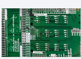
Definition and description of each layer:
1. TOP LAYER (top layer): Designed as the top layer of copper foil wiring. If it is a single-sided board, there is no such layer.
2. BOMTTOM LAYER (bottom wiring layer): Designed as bottom copper foil wiring.
3. TOP/BOTTOM SOLDER (top/bottom solder resist green oil layer): The top/bottom solder resist green oil is applied to prevent tin on the copper foil and maintain insulation. Open the window with solder mask at the pads, vias and non-electrical traces on this layer.
l In the design, the soldering pad will open a window by default (OVERRIDE: 0.1016mm), that is, the soldering pad exposes the copper foil and expands by 0.1016mm, and it will be tinned during wave soldering. It is recommended not to make design changes to ensure solderability;
l The via hole will be opened by default in the design (OVERRIDE: 0.1016mm), that is, the via hole exposes the copper foil and expands by 0.1016mm, and it will be tinned during wave soldering. If the design is to prevent the tin on the vias and not expose the copper, you must check the PENTING option in the additional properties of the vias SOLDER MASK (solder mask opening) to close the via opening.
l In addition, this layer can also be used for non-electrical wiring separately, and the solder mask green oil will open the window accordingly. If it is on a copper foil trace, it is used to enhance the overcurrent capability of the trace, and tin is added during soldering; if it is on a non-copper foil trace, it is generally designed for logo and special character silk screen printing, which can save production Character silk screen layer.
4. TOP/BOTTOM PASTE (top/bottom solder paste layer): This layer is generally used to apply solder paste during the SMT reflow process of SMT components, and has nothing to do with the printed board manufacturer's board. It can be deleted when exporting GERBER, PCB Just keep the default when designing.
5. TOP/BOTTOM OVERLAY (top/bottom screen printing layer): Designed for various screen printing logos, such as component tag numbers, characters, trademarks, etc.
6. MECHANICAL LAYERS (mechanical layer): Designed as PCB mechanical shape, the default LAYER1 is the shape layer. Other LAYER2/3/4, etc. can be used for mechanical size marking or special purposes. For example, when certain boards need to be made of conductive carbon oil, LAYER2/3/4, etc. can be used, but the purpose of the layer must be clearly marked on the same layer.
7. KEEPOUT LAYER (forbidden wiring layer): Designed as a forbidden wiring layer, many designers also use PCB mechanical appearance. If there are KEEPOUT and MECHANICAL LAYER1 on the PCB at the same time, it mainly depends on the completeness of the appearance of these two layers, generally MECHANICAL LAYER1 shall prevail. It is recommended to use MECHANICAL LAYER1 as the shape layer when designing. If you use KEEPOUT LAYER as the shape, do not use MECHANICAL LAYER1 to avoid confusion!
8. MIDLAYERS (middle signal layer): mostly used for multilayer boards, our company's design is rarely used. It can also be used as a special-purpose layer, but the purpose of the layer must be clearly marked on the same layer.
9. INTERNAL PLANES (internal electrical layer): used for multi-layer boards, our company design does not use.
10. MULTI LAYER (through hole layer): through hole pad layer.
11. DRILL GUIDE (drilling positioning layer): the center positioning coordinate layer of the pad and the hole drilling.