Today, it is difficult to design a high-speed electronic system without a thorough understanding of the chip, package structure, and PCB board power supply system characteristics. In fact, in order to meet the lower power supply voltage, signal flip faster, higher level of integration, and many more and more challenging demands, a lot of walking in the forefront of electronic design companies in product design process in order to ensure that the integrity of the power supply and signal, the analysis of power system into a lot of money, manpower and material resources.
The analysis and design of power supply systems (PDS) is becoming increasingly important in the field of high-speed circuit design, especially in the computer, semiconductor, communication, network and consumer electronics industries. With the inevitable further scaling down of VLSI technology, the supply voltage of integrated circuits will continue to decrease. As more and more manufacturers switch from 130nm to 90nm, we can expect the supply voltage to drop to 1.2V or even lower, while the current will increase significantly. From the perspective of DC IR voltage reduction to AC dynamic voltage fluctuation control, this development trend brings great challenges to the design of power supply systems due to the smaller and smaller allowable noise range.

PCB power supply system design overview
Usually in AC analysis, the input impedance between power sources and ground is an important observation to measure the characteristics of the power supply system. The determination of this observation in DC analysis evolves into the calculation of IR pressure drop. Whether in DC or AC analysis, the factors affecting the characteristics of the power supply system are: PCB layer, the shape of the power board layer plane, the layout of components, the distribution of holes and pins, and so on.
The concept of input impedance between power sources and ground can be used in the simulation and analysis of the above factors. For example, a very broad application of power supply ground input impedance is to evaluate the placement of decoupling capacitors on boards. With a certain number of decoupling capacitors placed on the board, the characteristic resonance of the board itself can be suppressed, thus reducing the generation of noise, and also reducing the edge radiation of the board to alleviate electromagnetic compatibility problems. In order to improve the reliability of power supply systems and the manufacturing cost of degraded systems, system design engineers must often consider how to economically and effectively choose the system layout of decoupling capacitors.
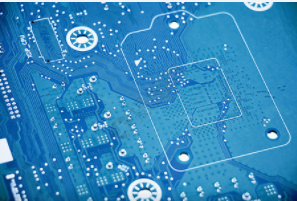
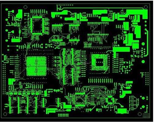
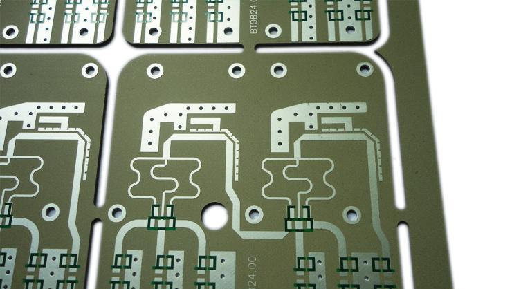
The power supply system in high-speed circuit system can be divided into three physical subsystems: chip, integrated circuit package structure and PCB. The power grid on the chip consists of alternating layers of metal. Each layer consists of strips of metal in the X or Y direction forming the power or ground grid. Holes connect the strips of metal in different layers.
For some high-performance chips, both the core and the IO power supply are integrated with many decoupling units. The integrated circuit package structure, like a miniature PCB, has several layers of intricately shaped power supplies or floor plates. On the upper surface of the package structure, the installation position of the decoupling capacitor is usually reserved. PCB usually contains continuous large power supply and floor plate, and some large and small discrete decoupling capacitor elements, and power rectifier module (VRM). Bond wires, C4 bumps and solder balls connect the chip, package and PCB together.
The entire power supply system should ensure that the integrated circuit components provide a stable voltage within the normal range. However, switching currents and parasitic high-frequency effects in those power supply systems will always introduce voltage noise.
In fact, it also reveals another very important fact, that the frequency range of the discrete decoupling capacitors placed on the PCB can only reach a few hundred megahertz. However high the frequency is, the parasitic inductance of each discrete decoupling capacitor and the loop inductance (capacitor to chip) of the board and through the hole will greatly reduce the decoupling effect. It is not possible to further reduce the input impedance of the power supply system only by placing discrete decoupling capacitors on the PCB. From several hundred megahertz to higher frequency ranges, the interplate capacitance of the power supply system of the package structure, as well as the discrete decoupling capacitance placed on the package structure, will come into play. In the GHz frequency range, the capacitors between the power grids in the chip and the decoupling capacitors in the chip are the decoupling solution.
In one example shown, the red line is the input impedance of a PCB after placing some discrete decoupling capacitors on it. Four resonant peaks appear at 600MHz to 700MHz. After taking into account the package structure, the inductance of the additional package structure moves the resonant peak to about 450MHz, as shown in the blue line. After the inclusion of the chip power supply system, the decoupling capacitor in the chip removes those high-frequency resonant peaks, but at the same time introduces a very weak resonant peak of 30MHz, as shown in the green line. This 30MHz resonance will be represented in the time domain as a voltage trough in the mid-frequency envelope of the high-frequency flipping signal.