PCB layout and design specifications that PCB design must know
We all know that "there is no rule, there can be no square circle", and the same is true of technology.
What specifications should be paid attention to in PCB design?
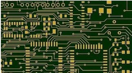
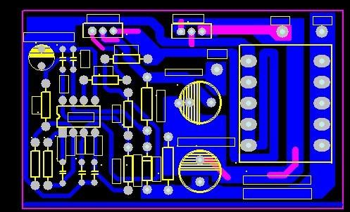
1. Layout design specification The distance from the edge of the board should be greater than 5mm=197mil. Place the components closely related to the structure, such as connectors, switches, power sockets, etc.
Priority should be given to core components and larger components of circuit function modules, and then priority to peripheral circuit components centered on core components.
Place high-power components in a position that is conducive to heat dissipation. E. Avoid placing high-quality components in the center of the circuit board and place them near the fixed edges of the chassis.
Components with high-frequency circuit board connections should be as close as possible to reduce the distribution of high-frequency signals and electromagnetic interference.

Keep input and output components as far away as possible During the debugging process, high-voltage components should be placed as far as possible where it is not easy to touch the pointer. The thermistor should be far away from the heating element. The layout of the adjustable element should be easy to adjust. Consider the signal flow direction and arrange the layout reasonably to make the signal flow direction as consistent as possible.
1. The layout should be even, neat and compact. SMT components should pay attention to the same orientation of the pads to facilitate assembly and soldering and reduce the possibility of bridging. The decoupling capacitor should be close to the power input. The height limit of each component on the wave soldering surface is 4mm. For PCBS with double-sided components, larger and denser ICs and plug-in components are placed on the top of the circuit board, while only smaller components and fewer pins and loosely arranged SMD components can be placed on the bottom.
Q: It is especially important to add the radiator to the small high-calorie components. Copper can be used to dissipate heat under high-power components, and thermal sensors should not be scattered around these components as much as possible. High-speed components should be as close as possible to the connector; digital circuits and analog circuits should be separated as much as possible, preferably grounded. The distance from the positioning hole to the nearby pad should not be less than 7.62mm (300mm), and the distance from the positioning hole to the edge of the surface mount device should not be less than 5.08mm (200mm).
2. Wiring design specifications The straight line should avoid sharp and right angles, and should be 45 degrees.
The signal lines of adjacent layers are orthogonal. High-frequency signals should be as short as possible
For input and output signals, try to avoid adjacent parallel lines. It is best to add a ground wire between the lines to prevent feedback coupling. The power and ground wires of the double panel should be aligned with the data stream to improve noise immunity.
Digital, similarly, separate H. The line width of the clock line and the high-frequency signal line should be considered according to the characteristic impedance requirements to achieve impedance matching. The wiring of the entire circuit board should be evenly perforated.
Single power layer and ground layer, power line and ground line should be as short and thick as possible, power and ground circuit should be as small as possible
Clock wiring should have as few perforations as possible, avoid parallel connection with other signal lines, keep away from general signal lines, and avoid interference with signal lines; at the same time, avoid the power supply on the circuit board to prevent interference between the power supply and the clock; when there are multiple clocks The frequency on the circuit board is different, and two clock lines with different frequencies cannot be connected in parallel.
The frequency clock is coupled to the output cable line and transmitted.
If there is a special clock generator chip on the circuit board, it cannot be routed underneath. Copper should be placed underneath. If necessary, it should be specially cut.
1. Pairs of differential signal lines are usually parallel to each other, with as few holes as possible. When drilling is required, the two wires should be pressed together to achieve impedance matching. When the distance between two solder joints is very small, the solder joints should not be directly connected; pull out from the board through the hole should be as far as possible from the pad.