Different points need to be set in different PCB design stages. In the layout stage, large grid points can be used for device layout.
For ICs, non-positioned connectors and other devices, a grid accuracy of 50-100 mils can be used for layout, while a grid of 25 mils can be used for passive small devices such as resistors, capacitors and inductors. The precision of the large dot matrix is conducive to the alignment and layout of the device.
PCB layout rules:
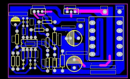
1. Under normal circumstances, all components should be placed on the same surface of the circuit board. Only when the top components are too dense, some devices with limited height and low heat output (such as chip resistors, chip capacitors, chip ICs) can be placed on the lower layer.
2. Under the premise of ensuring electrical performance, the components should be placed on the power grid and arranged side by side or vertically to maintain a clean and beautiful appearance. In general, overlapping components are not allowed; the components should be arranged in a compact manner and should be evenly distributed throughout the layout.
3. The minimum distance between the patterns of different components near the pads on the circuit board should be greater than 1mm.
4. The best shape of the circuit board is a rectangle with an aspect ratio of 3:2 or 4:3. When the surface size of the circuit board is larger than 200MM times 150MM, the mechanical strength of the circuit board should be considered.

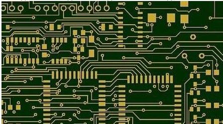
PCB layout design, PCB component analysis, layout design should be based on functions. When implementing the layout of all components of the circuit, the following principles should be followed:
1. Position each functional circuit unit according to the circuit flow to facilitate the signal flow, and keep the signal in the same direction as much as possible.
2. Pay attention to the core components of each functional unit and lay out around them. Components should be uniformly, integrally and compactly arranged on the PCB to minimize and shorten the leads and connections between components.
iPCB is a high-tech manufacturing enterprise focusing on the development and production of high-precision PCBs. iPCB is happy to be your business partner. Our business goal is to become the most professional prototyping PCB manufacturer in the world. Mainly focus on microwave high frequency PCB, high frequency mixed pressure, ultra-high multi-layer IC testing, from 1+ to 6+ HDI, Anylayer HDI, IC Substrate, IC test board, rigid flexible PCB, ordinary multi-layer FR4 PCB, etc. Products are widely used in industry 4.0, communications, industrial control, digital, power, computers, automobiles, medical, aerospace, instrumentation, Internet of Things and other fields.