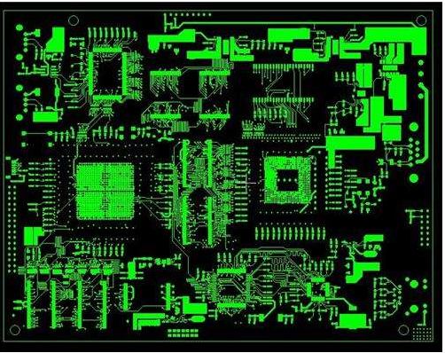
1. The main points of the final inspection of the circuit board design
In the electronics industry, there are many inexperienced PCB engineers. The design of the circuit board is usually because some checks are ignored at the end of the design, which leads to PCB board problems, such as insufficient line width, component labels silk-printed on the overpass, and the socket is too tight. Signal loop and so on. In turn, this can cause electrical problems or process problems, severely hitting the circuit board again, resulting in waste. One of the most important processes at the end of a circuit board design is inspection.
The final inspection of the circuit board design has many details:
1: Circuit board design component packaging
Spacer spacing
If it is a new device, you must draw your own component package to ensure proper spacing. The pad spacing directly affects the soldering of the component.

The size of the perforation (if any)
For plug-in equipment, the perforation size should reserve enough margin, usually not less than 0.2mm is appropriate.
Contour screen printing
The outline silk screen of the equipment is better than the actual size, which can ensure the stable installation of the equipment.
2: Board design layout
IC should not be near the edge of the circuit board
Equipment of the same module circuit should be placed nearby
For example, the decoupling capacitor should be close to the power pin of the IC, and the components of the same functional circuit should be placed in one area, layered to ensure the realization of the function.
Arrange the location of Siria according to the actual installation of the socket
According to the actual structure, the socket is led to other modules. For the convenience of installation, the approach principle is generally used to arrange the position of the socket, and it is usually close to the edge of the board.
Pay attention to the socket direction
The socket is in the correct direction and the direction is opposite, and the wire will be fixed again. For flat sockets, the socket direction should face the outside of the circuit board.
No equipment in restricted area
The source of interference should be far away from sensitive circuits
High-speed signals, high-speed clocks or high-current switching signals are sources of interference and should be kept away from sensitive circuits such as reset circuits and analog circuits. They can be separated by paving
2. Factors to consider when designing power plane PCB
The processing of the power plane plays an important role in PCB design. In a complete PCB design project, the usual power processing can determine the success rate of the project by 30%-50%. At this time, the basic elements that should be considered for power plane processing in the PCB design process are introduced.
1: When doing power processing, the first thing to consider is its current carrying capacity, which contains two aspects.
Is the width of the power cord or the width of the copper sheet sufficient? To consider the width of the power line, we must first understand the thickness of the copper layer of the power signal processing layer. The thickness of the copper layer of the PCB outer layer (TOP / BOTTOM layer) under the conventional process is 1OZ (35um), and the thickness of the inner copper layer According to the actual situation, it will reach 1OZ or 0.5OZ. For a copper thickness of 1OZ, under normal conditions, 20mil can carry a current of about 1A, and under a copper thickness of 0.5OZ, under normal conditions, 40mil can carry a current of about 1A.
Whether the size and number of holes in the layer change meet the power supply capacity. The first step is to understand the flow rate of a single perforation. Under normal circumstances, the temperature will rise to 10 degrees.
A 10mil through hole can carry a current of 1A, so in PCB design, if the power supply is 2A, use a 10mil through hole to punch the absorption layer, and there must be at least 2 through holes. Usually in PCB design, more holes are considered in the power supply channel to maintain a little margin.
PCB design
2: Second, we must consider the power supply path, specifically the following two aspects should be considered.
The power path should be as short as possible. If it goes too long, the power supply pressure drop will be more serious, and too much pressure drop will cause the project to fail.
The dynamic plane segmentation should be kept as long as possible in the rules, and no elongated rod and dumbbell-shaped segmentation are allowed.
When dividing the power supply, the separation distance between the power supply and the power plane should be kept as close as possible to about 20mil. If the area of the BGA part is large, a local distance of 10mil can be maintained. If the distance between the power plane and the aircraft is too close, there may be a risk of short circuit. .
If the power supply is processed in adjacent planes, please try to avoid parallel processing of copper sheets or lines. The main purpose is to reduce the interference between different power supplies, especially some voltage differences between power supplies. It is necessary to try to avoid the power plane overlap, which is difficult to avoid when the interval formation can be considered.
3: When doing power distribution, try to avoid the cross-segmentation of adjacent signal lines. When the signal is cross-segmented (the red signal line has cross-segmentation), the discontinuity of the reference plane will cause impedance mutations and EMI Crosstalk issues. In high-speed designs, crosstalk will have a great impact on signal quality.