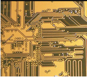
1. Impedance function of double-sided impedance circuit board
PCB impedance refers to the parameters of resistance and reactance, which hinder the conduction of alternating current. The impedance value is essential for some double-sided circuit boards with large currents. What are the specific effects of impedance on line circuit boards Several advantages: 1. After the PCB backplane is connected to the electronic components, issues such as conductivity and signal transmission performance need to be considered. At this time, the lower the impedance, the better.
2. The double-sided PCB board in the manufacturing process needs to go through multiple processes such as copper sinking, tin electroplating, and connector soldering. The materials used in each production link must ensure the low resistivity to ensure that the overall impedance of the PCB is low to meet the product quality requirements. normal operation. 3. PCB tin plating is the most prone to problems in the production of the entire circuit board, and it is also the key to the impedance. The biggest defect of the electroless tin layer is easy to change color (easy to be oxidized or deliquescent) and poor solderability, which will make the circuit board difficult to solder., Too high impedance leads to poor conductivity or unstable performance of the whole board.4. The conductors in the circuit board will transmit various signals. In order to increase its transmission rate, it is necessary to increase its frequency. If the circuit itself is different due to factors such as etching, stack thickness, wire width, etc., it is easy to cause the impedance to be worthwhile
1. The three most common methods for fpc soft and hard circuit board production

1: Process factors: copper foil is over-etched, electrolytic copper foil is usually single-sided galvanized (usually called ashing foil) and single-sided copper plating (usually called "red foil"), copper is generally galvanized above 70um Copper foil, red foil and fly ash foil below 18um basically have no batches of waste copper. When the data line design is better than the etching line, if the copper foil specification is changed and the etching parameters remain unchanged, the copper foil is in the etching solution The residence time in the medium will be too long. Zinc is originally an active metal. Soaking the copper wire on the PCB in the etching solution for a long time will inevitably lead to excessive side corrosion of the circuit, which will lead to some thin circuit backing zinc. The layer completely reacts and separates from the substrate, which is also called "copper wire shedding". (a) If there is no problem with the etching parameters of the PCB, but after the etchant is cleaned with water and dried, the copper wire is also surrounded by the residual etching liquid on the PCB circuit board. If it is not processed for a long time, it will produce copper wire, copper undercut and Too much dumping. This situation usually manifests as concentrated on thin circuits, or due to wet weather, similar defects will appear on the entire circuit board. Strip the copper wire to ensure the surface in contact with the base layer (the so-called rough surface) The color of) has been changed, which is different from the color of normal copper foil., The original copper color of the bottom layer is seen, and the peel strength of the copper foil at the thick line is also normal. (b) A local collision occurs during the circuit board production process, and the copper wire is separated from the base material under the action of external force. The poor performance is poor positioning or orientation. The copper wire will be obviously twisted, or there are scratches/impact marks in the same direction For example, if you peel off the copper wire at the defect site, look at the rough surface of the copper foil, the color of the rough surface of the copper foil is normal, there will be no side corrosion, and the peeling strength of the copper foil is normal.(C): The circuit design of the circuit board is unreasonable. If a thick copper foil is used to design a thin circuit, the circuit will be over-etched and the copper will be discarded.
2. Reasons for the lamination process: under normal circumstances, as long as the laminate is hot pressed for more than 30 minutes at a high temperature, the copper foil and prepreg are basically completely combined, so pressing usually does not affect the copper foil and laminate During the stacking and stacking process of laminates, if the PP is contaminated or the rough surface of the copper foil is damaged, the adhesion between the copper foil and the substrate after lamination will also be insufficient, resulting in positioning ( Only suitable for larger boards) or scattered copper wires fall off, but the peel strength of the copper wires near offline will not be abnormal. 3. Reasons for laminating raw materials: (a) As mentioned above, ordinary electrolytic copper foils are all products that are galvanized or copper-plated on wool. If the peak value of the wool foil is abnormal during the production process, or it is galvanized/galvanized/ When copper plating, the crystal branch of the plating layer is poor, and the peeling strength of the copper foil itself is insufficient. After the bad foil is pressed into the PCB board and inserted into the electronic factory, the copper wire will fall off due to external impact. This poor copper exclusion performance The copper wire will be peeled off, and looking at the rough surface of the copper foil (that is, the surface in contact with the substrate), there is no obvious side corrosion, but the peel strength of the entire copper foil will be very poor. (b) The adaptability of copper foil and resin is poor: now some laminates with special properties are used, such as HTg board. Due to different resin systems, the curing agent used is usually PN resin, and the resin molecular chain structure is simple and the degree of crosslinking is low., It is necessary to use copper foil with special peaks to match. In the production of laminates, the use of copper foil does not match the resin system, resulting in insufficient peel strength of the metal foil of the metal-clad laminate, and poor copper wire shedding during insertion.