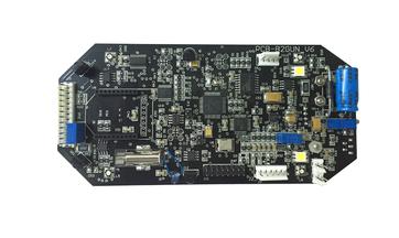
PCB circuit board power plane processing
The processing of the power plane has a key influence in the design of the PCB circuit board. In a detailed design project, the processing of the power supply can usually determine the success rate of the project by 30% to 50%. This time I will give you a detailed introduction to the power plane processing in the PCB circuit board design process. The basic elements.
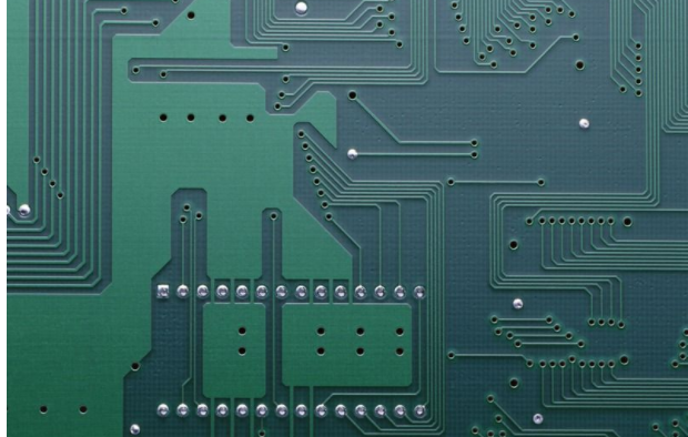
Current carrying capacity
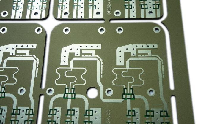
Whether the power line width or copper spacing is sufficient. It is necessary to fully consider the power line width. The premise is to understand the copper thickness of the layer where the power signal is processed. The copper thickness of the outer layer (TOP/BOTTOM layer) of the PCB circuit board under the conventional process is 1OZ (35um), and the copper thickness of the inner layer will follow Its actual use is 1OZ or 0.5OZ. For 1OZ copper thickness, under normal circumstances, 20mil can carry a current of about 1A; 0.5OZ copper thickness, under normal circumstances, 40mil can carry a current of about 1A.
Whether the size and number of holes meet the power supply current capacity when changing layers.
Power path
The power path should be as short as possible. If it goes too long, the power loss will be more serious, and the loss will cause the project to fail.

The division of the power plane should be as regular as possible, and slender and dumbbell-shaped divisions are not allowed.
Power split
When dividing the power supply, keep the separation distance between the power supply and the power plane as close as possible to about 20 mils. Assuming that in some areas of the BGA, the separation distance of 10 mils can be locally maintained. If the distance between the power plane and the plane is too close, there is a risk of short circuit. .
If the power supply is handled on the adjacent plane, avoid the copper skin or parallel processing of the traces as much as possible. The main purpose is to reduce the interference between different power supplies, especially between power supplies with very different voltages. The overlap of power planes must be avoided as much as possible. If it is unavoidable, the intermediate ground can be fully considered.
When doing power splitting, avoid the cross-segmentation of adjacent signal lines as much as possible. The signal will cause impedance mutations due to the discontinuity of the reference plane at the cross-segmentation position, which will cause EMI and crosstalk problems. The signal quality has a great influence.
Classification of coating (plating) coating on the surface of PCB circuit board
1. Classified by processing technology (coating or plating)
According to the processing method, it can be divided into two categories: surface coating and metal surface coating.
• PCB surface coating
Surface coating refers to the physical coating of a thin layer of heat-resistant and solderable coating on the surface of the latest copper lands. For example, the natural rosin selected from the beginning, various artificial rosin substances (including various fluxes) to OSP (organic solderability preservative). These main features are to protect and produce the latest (non-pollution and non-oxidation) copper surface to provide solder direct connection before soldering and during the whole soldering process. Hot-air solder leveling (HASL) is also coated, but it begins to produce "temporary steady state" CuxSny intermetallic compound (IMC) during the whole process of HASL. The solder is soldered to the CuxSny IMC.
• PCB metal surface plating layer
The metal surface coating refers to a thin layer of heat-resistant and solderable metal coating on the surface of the latest copper connection plate by electroless plating or electroplating, such as electroplating gold, electroless tin plating, electroless silver plating, and electroless nickel plating -Gold, electroless nickel-palladium-gold, electroless nickel-palladium, electroless palladium, etc. These main features are to protect and produce the latest (non-pollution and non-oxidation) copper surface or metal barrier layer before soldering and during the entire welding process to ensure that the solder can be soldered on the copper surface or barrier layer surface.
2. Classified by application effect
According to the application (welding) results, these surface coating (plating) coatings can be divided into three categories: (1) the surface coating (plating) coating of solder soldering on the non-resistive barrier layer; (2) the soldering solder spreading The metal surface plating layer on the layer; (3) The metal surface plating layer soldered on the barrier layer.
• The surface coating (plating) coating on the non-resistive barrier layer by soldering
The main feature of this type of surface coating (plating) coating is that it is squeezed away from the copper surface by the molten solder during the entire process of high-temperature soldering and floats on the solder surface or thermally decomposes or both are removed, but the connection interface of the solder joint will be removed. Produce transiently stable intermetallic compounds (IMC), leading to potential failures during the entire application process, such as natural rosin, artificial rosin (including various fluxes), OSP (organic solderability preservative) ), electroless tin plating, electroless silver plating and so on.
• Surface plating layer of solder on the diffusion layer
In order to remove the transiently stable intermetallic compound (IMC), thick gold-plated copper was initially used as the surface coating. However, practice and application have shown that: (1) Gold-copper is prone to diffusion between each other, that is, gold Atoms will diffuse into the copper crystal structure, and copper atoms will also diffuse into the gold crystal structure. This is also because gold and copper are all face-centered cubic crystals, and their melting points and atomic radii are very similar, so diffusion is easy to occur; ( 2) The diffusion layer between the gold-copper interface is prone to internal stress. This is also because the thermal expansion coefficient of copper is greater than the thermal expansion coefficient of gold. The crystalline structure of the diffused gold-copper interface will inevitably produce internal stress caused by mutual extrusion. It will become loose, brittle, and other problems, resulting in PCB circuit failure.
•The surface metal plating layer of the welding material welded on the barrier layer
The specific characteristics of this surface coating layer are: during the high temperature welding process, the welding material is welded on the surface of the metal barrier layer, rather than immediately PCB welding on the copper surface. Therefore, it is impossible to produce at the connection interface of the solder joint. Unstable intermetallic compounds, and it is impossible to diffuse between metals: such as electroplating nickel-gold, electroless nickel-gold, electroless nickel-palladium-gold, electroless nickel-palladium, electroless palladium, etc. Because the barrier layer is metal and all produced by electroless plating or electroplating, it can also be called a metal surface plating layer.