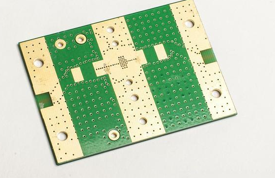
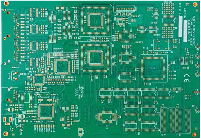
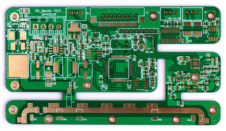
With the rapid development of electronic technology and the wide application of wireless communication technology in various fields, high frequency, high speed, and high density have gradually become one of the significant development trends of modern electronic products. High-frequency and high-speed digitization of signal transmission force PCB to micro-hole and buried/blind hole, fine conductor, medium layer uniform thin, high frequency, high-density multilayer PCB design technology have become an important research field. Based on years of experience in hardware design, the author summarizes some design skills and matters needing the attention of high-frequency PCB for your reference.

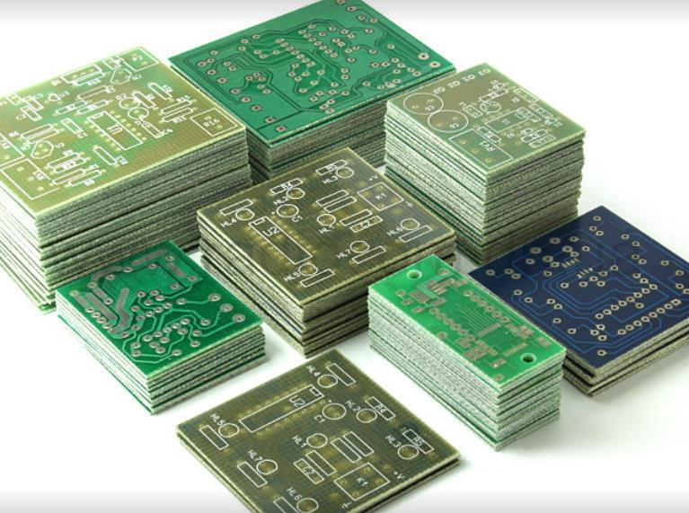
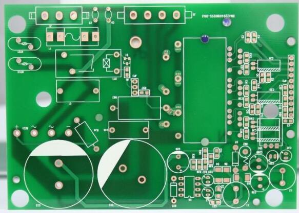
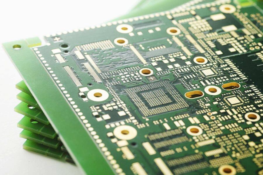
1. How to select the PCB sheet?
Selecting PCB boards must strike a balance between satisfying design requirements, mass production, and cost. The design requirements include both electrical and mechanical components. This material issue is usually important when designing very high-speed PCB board (frequencies greater than GHz). For example, the current commonly used FR-4 material, in the frequency of several GHz dielectric loss (dielectric loss) can have a great impact on signal attenuation, may not be suitable. For electrical purposes, pay attention to the dielectric constant, and dielectric loss at the designed frequency is appropriate.
2. How to avoid high-frequency interference?
The basic idea of avoiding high-frequency interference is to minimize the interference from the electromagnetic field of high-frequency signals, known as Crosstalk. They can be used to lengthen the distance between the high-speed signal and the analog signal or to add ground guard/shunt traces besides the analog signal. Also, pay attention to the noise interference of digital ground to analog ground.
3. How to solve the problem of signal integrity inhigh-speed design?
Signal integrity is a matter of impedance matching. The factors that affect the impedance match include the signal source structure and output impedance, the characteristic impedance of the cable, the characteristics of the load side, and the topology of the cable. The solution is by termination and adjusting the topology of routing.
4. How is the differential wiring implemented?
Differential wiring has two points to pay attention to, one is that the length of the two lines should be as long as possible, the other is that the distance between the two lines (which is determined by the differential impedance) should always remain the same, that is, to keep parallel. There are two parallel ways: one is that two lines are running side-by-side on the same layer, and the other is that two lines are running over-under under two adjacent layers. The former side-by-side(side by side, side by side) is more common.
5, for only one output of the clock signal line, how to achieve differential wiring?
It only makes sense to use differential wiring if both the source and the receiver are differential signals. So it is not possible to use differential wiring for a clock signal with only one output.
6. Can a matching resistor be added between the differential line pairs at the receiving end?
The matching resistance between the differential line pairs at the receiving end is usually added and should be equal to the value of the differential impedance. You'll get a better signal quality.
7. Why should the wiring of differential pairs be close and parallel?
Wiring for differential pairs should be properly close and parallel. The proper proximity is because the distance will affect the value of the differential impedance, which is an important parameter in the design of different pairs. Parallelization is also needed to maintain consistency in the differential impedance. If the two lines are closer or farther, the differential impedance is inconsistent, which affects signal integrity and timing delay.
8. How to deal with some theoretical conflicts in actual wiring?
The modular/digital separation is right. Attention should be paid to the signal routing as far as possible not to cross the moAT, and do not let the supply and signal returning current path become too large.
The crystal oscillator is a simulated positive feedback oscillation circuit. To have a stable oscillation signal, it must meet the specifications of loop gain and phase. However, the oscillation specifications of this simulated signal are easy to interfere with, even if ground guard traces are added, the interference may not be completely isolated. And too far away, the noise in the ground plane will also affect the positive feedback oscillation circuit. Therefore, be sure to bring the distance between the crystal oscillator and the chip as close as possible.
There are indeed many conflicts between high-speed cabling and EMI requirements. But the basic principle is that because of the resistance-capacitance or Ferrite Bead added by EMI, some electrical characteristics of the signal cannot be caused to not meet the specification. Therefore, it is best to solve or reduce EMI problems by arranging wiring and PCB layering techniques, such as high-speed signal layering. Finally, resistance-capacitance or Ferrite Bead was used to reduce the damage to the signal.
9. How to solve the contradiction between manual wiring and automatic wiring of high-speed signals?
Most of today's strong cabling software's automatic cablers have set constraints to control the winding mode and the number of holes. EDA companies sometimes have vastly different winding engine capabilities and constraint setting projects. For example, whether there are enough constraints to control how serpentine snakes, whether the spacing of differential pairs can be controlled, etc. This will affect the way the automatic wiring out of the wiring can conform to the designer's idea. In addition, the difficulty of manually adjusting the wiring is related to the ability of the winding engine. For example, the pushing ability of the wire, the pushing ability of the hole, and even the pushing ability of the wire to the copper, etc. Therefore, the choice of a strong cabling engine capability is the solution.
10. Test coupon.
The Test coupon is used to measure whether the characteristic impedance of the manufactured PCB meets the design requirements by using Time Domain Reflectometer (TDR). Generally to control the impedance has a single line and difference on two cases. Therefore, the line width and line spacing (with differential pairs) on the test coupon should be the same as the line to be controlled. The most important thing is the position of the ground point at the time of measurement. To reduce the inductance of the ground lead, the grounding place of the TDR probe is usually very close to the probe tip of the measuring signal. Therefore, the distance between the measuring signal point and the grounding point on the test coupon should be consistent with the used probing rod.
11. Can we use the microstrip line model to calculate the characteristic impedance of the signal line above the power plane? Can the signal between the power supply and the ground plane be calculated using the stripline model?
Yes, both the power plane and the ground plane must be considered reference planes when calculating the characteristic impedance. For example, four layers of plate: top layer - power layer - stratum - bottom layer. At this time, the model of the top layer routing characteristic imped nce is the microstrip line model with the power plane as the reference plane.
12. In high-speed PCB design, the blank area of the signal layer can be coated with copper, but how to distribute the copper of multiple signal layers on grounding and power supply?
In general, the copper application in the blank area is mostly grounded. Only in the high-speed signal line when applying copper should pay attention to the copper and signal line distance, because the copper will reduce the characteristic impedance of the line a little. It is also important not to affect the characteristic impedance of its layer, such as in the dual stripline structure.