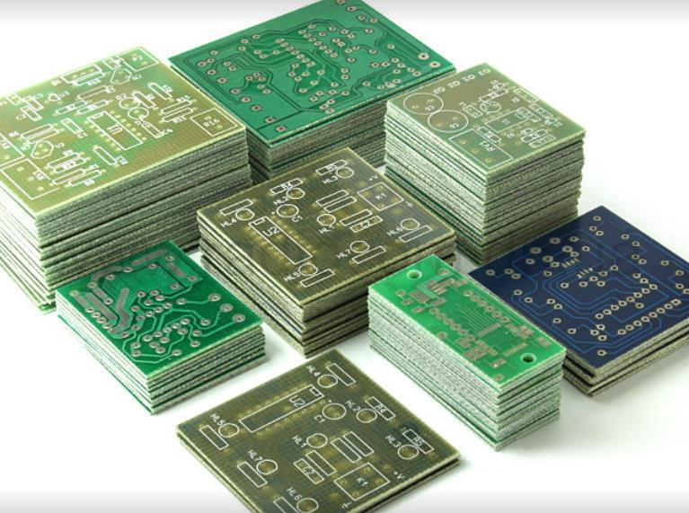
With the rapid development of electronic technology and the wide application of wireless communication technology in various fields, high frequency, high speed, and high density have gradually become one of the significant development trends of modern electronic products.High-Frequency PCB Circuit of signal transmission force PCB to micro-hole and buried/blind hole, fine conductor, medium layer uniform thin, high frequency, high-density multilayer PCB design technology have become an important research field. Based on years of experience in hardware design, the author summarizes some design skills and matters needing the attention of high-frequency circuits for your reference.

25. How to achieve EMC requirements as much as possible without causing too much cost pressure?
The increased cost of EMC on PCB board is usually due to the increase of the number of layers to enhance shielding effect and the increase of Ferrite Bead, Choke, and other high-frequency harmonic suppression devices. In addition, it is usually necessary to combine shielding structures on other mechanisms to make the entire system pass EMC requirements. The following are just a few design tips for PCB board to reduce the electromagnetic radiation effects produced by circuits.
The devices with a slower signal rate are selected as far as possible to reduce the high-frequency components produced by the signal.
Pay attention to the location of high-frequency devices. Do not place them too close to external connectors.
Pay attention to impedance matching of high-speed signals, the cabling layer, and its return current path to reduce high-frequency reflection and radiation.
Place sufficient and appropriate decoupling capacitors on the power pins of each device to mitigate the noise on the power layer and the formation. Pay special attention to whether the frequency response and temperature characteristics of the capacitor meet the design requirements.
26. when a PCB board has more than one number/module function block, the conventional practice is to separate the number/module, why?
The reason for the separation of digital/mode ground is that the digital circuit generates noise in power and ground when switching between high and low potentials. The size of the noise depends on the speed of the signal and the size of the current. If the ground plane is not divided and the noise generated by the digital area circuit is large while the analog area circuit is very close, the analog signal will still be disturbed by the ground noise even if the digital and analog signals do not cross. That is to say, the digital and analog undivided mode can only be used when the analog circuit area is far away from the digital circuit area that produces large noise.
27. Another way is to ensure that the number/module separate layout and the number/module signal line do not cross each other, the whole PCB board is not divided, the number/module is connected to the ground plane. Why?
The requirement that analog signals cannot cross the wires is that the return current path of a faster digital signal will try to flow back to the source of the digital signal along the ground near the bottom of the cable. If the analog signal crosses the wires, the noise generated by the return current will appear in the analog circuit area.
28. How to consider the impedance matching problem when designing the schematic diagram of high-speed PCB design?
Impedance matching is one of the key elements in designing the high-speed PCB circuit. The impedance value is related to the routing mode. For example, the distance between the surface layer (microstrip) or the inner layer (stripline/double stripline), the reference layer (power layer or stratum), the cable width, and the PCB material will all affect the characteristic impedance value of the routing. That is to say to determine the impedance value after wiring. General simulation software will be due to the line model or the limitations of the mathematical algorithm used to consider some impedance discontinuous wiring situation, at this time in the schematic diagram can only reserve some terminators, such as series resistance, to mitigate the effect of impedance discontinuous wiring. The real fundamental solution to the problem or wiring as far as possible is to avoid impedance discontinuous occurrence.
29. Where can I provide a more accurate IBIS model base?
The accuracy of the IBIS model directly affects the simulation results. IBIS can be regarded as the electrical characteristic data of the equivalent circuit of the I/O buffer of the actual chip, which can be converted by the SPICE model (or measured, but there are more restrictions). However, SPICE data is related to chip manufacturing, so the same device is provided by different chip manufacturers. The SPICE data is different, and the data in the transformed IBIS model will be different. That is to say, if manufacturer A's devices are used, only they can provide accurate model data for their devices because no one else will know better than them what process their devices are made by. If the IBIS provided by the vendor is not accurate, the only fundamental solution is to constantly ask the vendor to improve it.
30. In the design of high-speed PCB, which aspects should the designer consider the rules of EMC and EMI?
Generally, EMI or EMC design needs to consider both radiated and conducted aspects. The former belongs to the higher frequency part (> 30MHz) the latter is the lower frequency portion (< 30 MHZ). So you can't just focus on the high frequencies and ignore the low frequencies. A good EMI/EMC design must be considered at the beginning of the layout of the device position, PCB lamination arrangement, important online route, device selection, etc., if these do not have a better arrangement in advance, the solution will be less effective, increase the cost. For example, the position of the clock generator should not be close to the external connector as far as possible, the high-speed signal should go to the inner layer as far as possible and pay attention to the continuity of the characteristic impedance matching and the reference layer to reduce the reflection, the slope of the signal driven by the device should be as small as possible to reduce the high-frequency component, When selecting a decoupling/bypass capacitor, pay attention to whether the frequency response meets the requirements to reduce the power layer noise. In addition, pay attention to the high-frequency signal current backflow path to minimize the loop area (i.e. the loop impedance) to reduce the radiation. The range of high-frequency noise can also be controlled by dividing the formation. Finally, the chassis ground between THE PCB and the chassis is selected appropriately.
31. How to choose EDA tools?
In current PCB design software, thermal analysis is not a strong point, so it is not recommended to use it. As for other functions, 1.3.4 PADS or Cadence can be selected, both performance and cost are good. PLD design beginners can use the integrated environment provided by PLD chip manufacturers, in the design of more than a million doors can choose a single point tool.
32. Please recommend an EDA software suitable for high-speed signal processing and transmission.
For general circuit design, INNOVEDA PADS are very good, and they are compatible with simulation software, which often accounts for 70% of the applications. For high-speed circuit design, analog and digital hybrid circuits, using Cadence solution is the best software for performance and price, of course, Mentor performance is very good, especially its design process management should be the best. (Datang Telecom technical expert Wang Sheng)
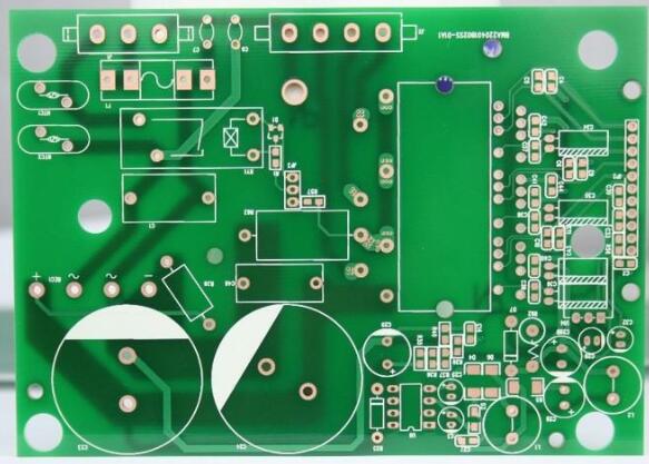
33. The interpretation of the meanings of each layer of PCB board?
Topoverlay- The name of a top layer component, also called Top Silkscreen or Top Component Legend, such as R1, C5,IC10. Bottomoverlay -- same thing as multilayer-- if you design a 4 layer board and you put a free pad or via, define it as multiply then its pad automatically appears on all 4 layers, If you just define it as the top layer, then its pad will only appear on the top layer.
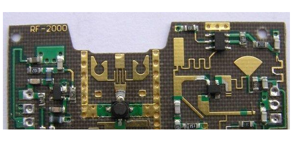
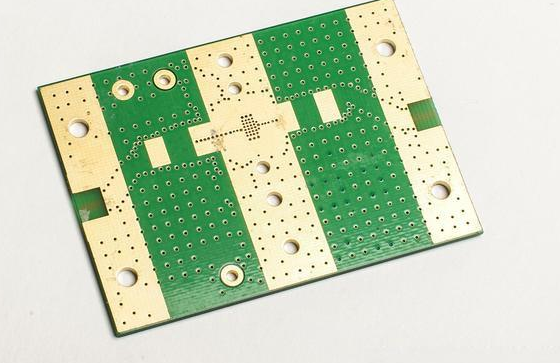
34. What should be paid attention to in the design, routing, and typesetting of high-frequency PCB above 2G?
Above 2G high-frequency PCB belongs to rf circuit design, not within the scope of high-speed digital circuit design. The layout and routing of the RF circuit should be considered together with the schematic because the layout and routing will cause distribution effects. In addition, rf circuit design some passive devices are realized by parameterizing the definition of special shape copper foil, so the EDA tool is required to provide parametric devices that can edit special shape copper foil. Mentor BoardStation has dedicated RF design modules to meet these requirements. In addition, the general RF design requires specialized RF circuit analysis tools, the most famous of which is Agilent's Eesoft, which has a good interface with Mentor's tools.
35. For all digital signal PCB, the board has an 80MHz clock source. In addition to the wire mesh (grounding), what kind of circuit protection should be used to ensure sufficient driving capacity?
Ensure that the clock drive capability, should not be achieved through protection, generally using a clock driver chip. The common concern about clock drive capability is because of multiple clock loads. Adopt clock driver chip, turn one clock signal into several, adopt point-to-point connection. Select the driver chip, in addition to ensuring that the basic match with the load, the signal along with the requirements (generally clock along with the effective signal), in the calculation of the system timing, to calculate the clock in the driver chip delay.