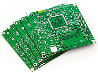
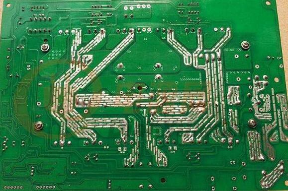
With the rapid development of electronic technology and the wide application of wireless communication technology in various fields, high frequency, high speed, and high density have gradually become one of the significant development trends of modern electronic products. High-frequency and high-speed digitization of signal transmission force PCB to micro-hole and buried/blind hole, fine conductor, medium layer uniform thin, high frequency, high-density multilayer PCB design technology have become an important research field. Based on years of experience in hardware design, the author summarizes some design skills and matters needing the attention of high-frequencyPCB circuits for your reference.

36. In the digital and analog co-existing system, there are two processing methods. One is the separation of digital and analog ground, for example, in the stratum, the digital ground is an independent piece, and the analog ground is an independent piece. The other is that the analog power supply and the digital power supply are connected separately with FB, and the ground is unified. Mr. Li, do these two methods have the same effect?
I should say it's the same in principle. Because power and ground are equivalent for high-frequency signals. The purpose of distinguishing the analog and digital parts is to prevent interference, mainly the interference of the digital circuit to the analog circuit. However, the segmentation may result in an incomplete backflow path, which affects the signal quality of digital signal and EMC quality. Therefore, no matter which plane is divided, it is necessary to see whether the signal backflow path is enlarged and how much the backflow signal interferes with the normal working signal. Now there are some hybrid designs, regardless of power and ground, in the layout, according to the digital part, the analog part of the layout of separate wiring, to avoid the presence of cross-zone signals.
37. If a separate clock signal board is used, what kind of interface is generally used to ensure that the transmission of the clock signal is less affected?
The shorter the clock signal, the smaller the transmission line effect. The use of a separate clock signal board will increase the length of signal wiring. And the grounding power supply of the board is also a problem. If the long-distance transmission is required, differential signals are recommended. LVDS signals can meet drive capability requirements, but your clock is not too fast to be necessary.
38. 27M, SDRAM clock line (80m-90m), the second and third harmonics of these clock lines are just in the VHF band, and the interference is very large after being docked from the high-frequency PCB Circuit of the receiving end. In addition, to shorten the length of the line, there are other good ways?
If the third harmonic is large and the second harmonic is small, it might be because the duty cycle of the signal is 50%, because in that case, the signal has no even harmonics. The signal duty cycle needs to be modified. In addition, if the clock signal is unidirectional, the source-end series matching is generally adopted. This suppresses the secondary reflection but does not affect the clock edge rate. The matching value of the source can be obtained by using the following formula.
39. What is the routing topology?
Topology, also known as routing order, is the routing order for a network with multiple ports.
40. How to adjust the cabling topology to improve signal integrity?
This kind of network signal direction is complicated because the influence of topologies on unidirectional and bidirectional signals and signals of different level types is different, it is difficult to say which topologies are beneficial to signal quality. What kind of topology is required for engineers to understand the circuit principle, signal type, and even the difficulty of wiring when making pre-simulation.
41. How to reduce EMI problems by layering?
First of all, EMI should be considered from the system, PCB alone can not solve the problem. In terms of EMI, I think the main purpose of stacking is to provide the shortest signal backflow path, reduce the coupling area and suppress the differential mode interference. In addition, the tight coupling between the formation and the power layer and appropriate epitaxy of the power layer is beneficial to the suppression of common-mode interference.
42. Why copper?
There are several reasons for laying copper in general. EMC. For a large area of the ground or power supply copper, will play a shielding role, some special, such as PGND plays a protective role. PCB process requirements. In general, in order to ensure the electroplating effect, or laminate without deformation, for the wiring less PCB layer copper. Signal integrity requirements, give the high-frequency digital signal a complete backflow path, and reduce the dc network wiring. Of course, there are heat dissipation, special device installation requirements copper, and so on.
43. In a system, including DSP and PLD, may I ask the wiring should pay attention to what problems?
Look at the ratio of your signal rate to the length of your wiring. If the delay of the signal on the transmission line is comparable to the variation of the signal over time, the problem of signal integrity should be considered. In addition, for multiple DSPS, clock, and data signal routing topology will also affect signal quality and timing, which needs to be paid attention to.
44. In addition to the protel tool wiring, there are other good tools?
As for tools, in addition to protelL, there are many wiring tools, such as mentor's WG2000, EN2000 series and power PCB, cadence's Allegro, Zuken's Can star, CR5000, and so on, each has its own strengths.
45. What is a "signal backflow path" ?
Signal reflux path, that is, return current. When a high-speed digital signal is transmitted, the direction of the signal is from the driver along the PCB transmission line to the load, and then from the load along the ground or power supply through the shortest path back to the driver. This return signal on the ground or power supply is called the signal backflow path. In his book, Dr.Johson explains that high-frequency signal transmission is actually the process of charging the dielectric capacitor that is wrapped between the transmission line and the DC layer. SI analyzes the electromagnetic properties of the paddock and the coupling between them.
46. How to interconnect with plug-ins for SI analysis?
The connector model is described in the IBIS3.2 specification. EBD model is generally used. For special boards, such as backplanes, SPICE models are required. You can also use multi-board simulation software (HYPERLYNX or IS_multiboard) to set up a multi-board system by inputting the distribution parameters of connectors, which are generally obtained from the connectors manual. Of course, it's not precise enough, but as long as it's acceptable.
47. What are the terminals?
Terminal, also known as a match. Generally, the matching position is divided into active end matching and terminal matching. The source end matching is generally resistor series matching, and the terminal matching is generally parallel matching. There are many ways, such as resistor pull-up, resistor pull-down, Davinen matching, AC matching, and Schottky diode matching.
48. What factors determine the use of the end (matching)?
The matching model is generally determined by the buffer characteristic, top condition, level type, and decision mode. Signal duty cycle and system power consumption should also be considered.
49. What are the rules for using the end (match) method?
The most important problem of the digital circuit is timing. The purpose of adding matching is to improve the signal quality and get a definite signal at the decisive moment. For the level of the effective signal, the signal quality is stable on the premise of ensuring the establishment and holding time. On the premise of ensuring the monotonicity of the signal, the variation speed of the signal can meet the requirements. The Mentor ICX product textbook has information about matching. In addition, High-Speed Digital Design a Hand Book of BlackMagic has a chapter dedicated to the terminal, which describes the role of matching on signal integrity from the principle of electromagnetic wave, for reference.
50. Can the logic function of the device be simulated by using the IBIS model of the device? If not, how do you perform board-level and system-level simulations of the circuit board?
The IBIS model is a behavior-level model and cannot be used for functional simulation. For functional simulation, you need SPICE models, or other structural level models.