Status of Advanced Substrates 2018: Embedded Dies & Interconnects, Substrates Like PCB Trends
Apple has adopted Substrate-Like PCB (SLP) in its latest iPhone 8 and iPhone X, which may revolutionize the substrate and PCB market.
Advanced substrates need to take into account process size reduction and functional requirements
The development trend of the semiconductor industry is affecting the semiconductor packaging technology and the degree of interconnection from the package to the circuit board. Performance-driven applications such as personal computers and smartphones are making way for functional applications that guide the future development of the semiconductor industry, such as the Internet of Things, automobiles, 5G interconnection, AR/VR (augmented reality/virtual reality) and artificial intelligence (AI) Etc. The massive data processing spawned by various new applications is also critical, which means that better data processing performance and reduction in the size of the semiconductor process will continue to be the driving engine of the semiconductor industry.
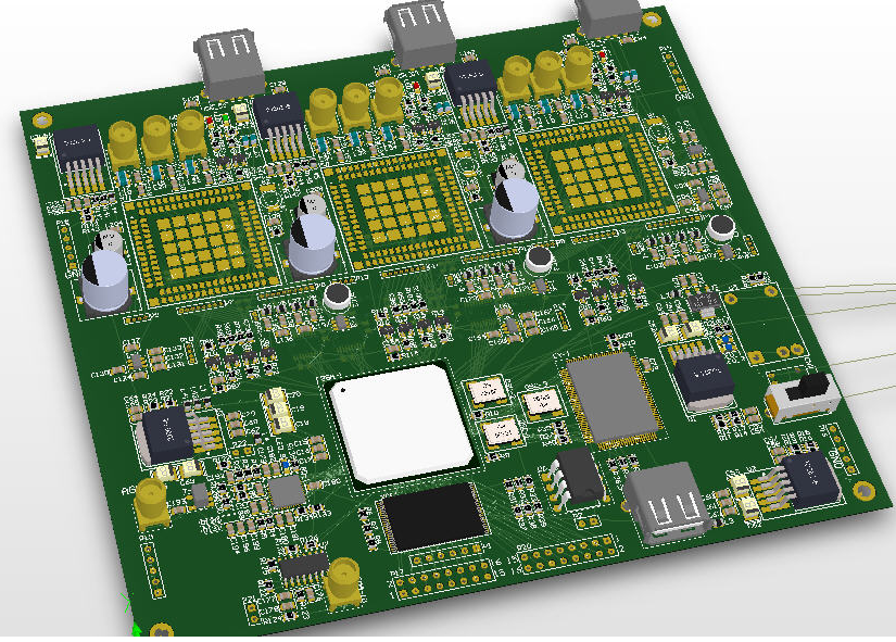
Advanced semiconductor packaging technology has become an effective way to increase the value of semiconductor products by increasing product functionality, maintaining/improving performance and reducing costs. For this reason, PCB is no longer just a connector, but an integrated solution.
Line width opportunities for PCB/substrate manufacturers
On the development roadmap of the shrinking semiconductor process size, three active competition areas have been formed under the line width (L/S) 30/30um:
-Circuit board vs.package substrate(L/S 30/30 um ~ L/S 20/20um): It is developing towards substrate type PCB;
-Package substrate vs. No substrate (fan-out type) (L/S 10/10um and below): Flip-chip substrates, embedded chips in panel-level packaging (PLP) substrates, are competing with fan-out wafer-level packaging Compete with panel-level packaging;
-Through silicon via (TSV) packaging vs. no through silicon via alternative packaging technology (L/S 5/5 um to L/S 1/1 um and below): 2.5D (such as silicon interposer) packaging vs. high density Fan-out package
The functional development roadmap of advanced substrates is related to devices that do not focus on interconnection expansion requirements, but must meet specific requirements such as high frequency, high reliability, and high power. These advanced package types include 5G millimeter wave RF SIP (Radio Frequency System-in-Package) and embedded chips in substrates for high-reliability/high-power applications. This report pays special attention to substrate-based PCBs and embedded chips in substrates, and deeply studies the entire PCB and IC substrate (FC CSP/FC BGA) industries.

Substrate PCB: the collision of two technologies
Driven by Apple and its iPhone 8/iPhone X, the process in high-end smartphones is transitioning from subtractive to mSAP (modified semi-additive), and PCB is transitioning to substrate-based PCB. Other high-end smartphone suppliers such as Samsung and Huawei are also expected to follow suit in the near future.
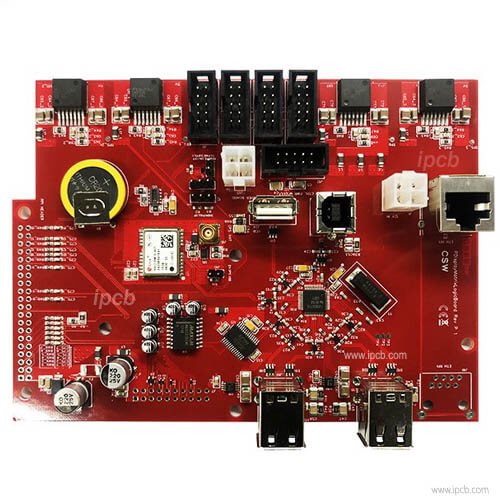
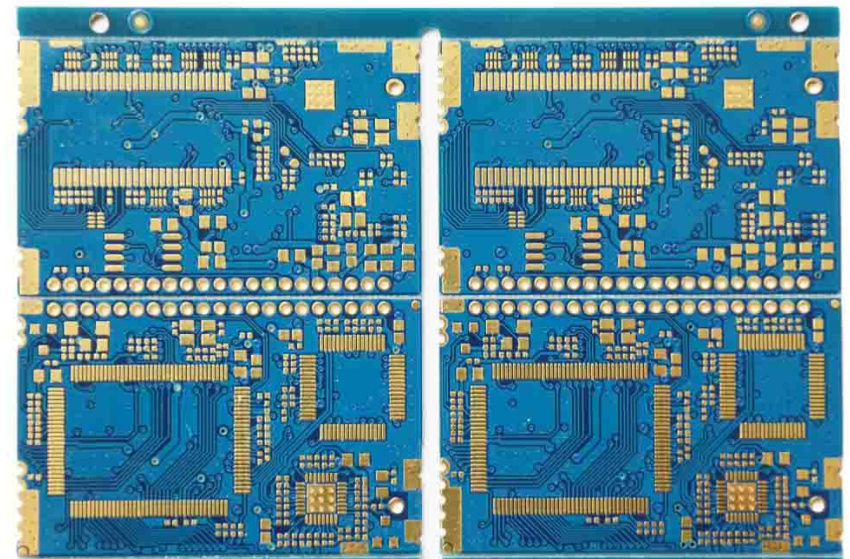
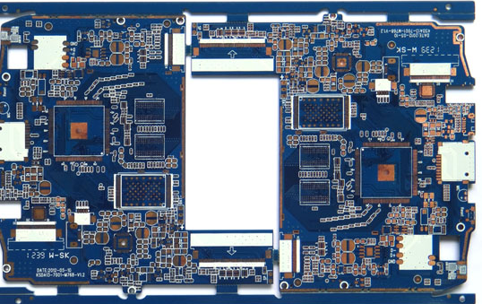
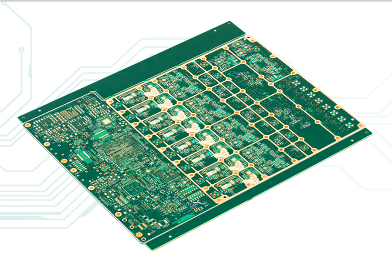
Substrate type PCB means that the circuit board in the product is gradually turning to have characteristics similar to the package substrate. Standard HDI and non-HDI circuit boards use a modified subtractive manufacturing process, while packaging substrates (such as FC/WB CSP/BGA) use mSAP or SAP processes. Substrate PCB is actually a large-scale substrate manufactured by mSAP process with circuit board size and functions. Substrate-based PCBs have higher line resolution, better electrical performance, and potential energy consumption and size advantages than standard or HDI circuit boards, which are very important for smartphones with limited space and energy consumption.
The emergence of substrate PCB has opened up a whole new market and will change the current supply chain. As shown in the figure below, the size of the substrate PCB market is expected to be US$190 million in 2017, and is expected to grow to US$2.24 billion by 2023, with a compound annual growth rate of 64% during 2017-2023. Substrate-based PCB manufacturing will not only stimulate the recovery of the substrate market, but will also promote substantial growth in this market. However, from the perspective of technological maturity, although the mSAP process has matured to process packaging substrates, there are still great challenges for manufacturing PCB-sized substrates.
This report provides a comprehensive and in-depth study of the entire substrate PCB market, covering the entire supply chain, and provides a technical comparison between the subtractive method/mSAP/SAP process, as well as the dismantling comparison of iPhone 8, iPhone X and Samsung S8 .
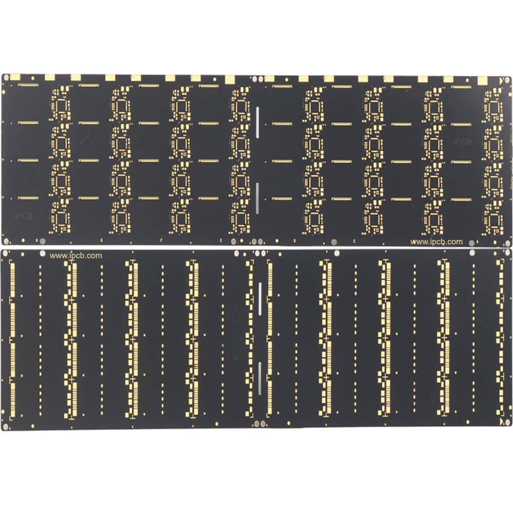
With the emergence of substrate-based PCBs in Apple’s latest iPhone, PCB and substrate manufacturers have begun to manufacture substrate-based PCBs and invest in mSAP. The 28 PCB/substrate manufacturers selected in this report are believed to have mastered substrate-based PCB technology, and some of them have been able to manufacture substrate-based PCBs in batches.
Driven by high-end smartphones, some manufacturers have begun to invest heavily. At the same time, some large manufacturers have shown stable revenue in their PCB/substrate business. This report provides detailed information on the financial performance of these manufacturers in PCB/substrate manufacturing and other aspects.
Embedded chip packaging cost considerations
In order to achieve differentiated competition in the highly competitive PCB/substrate market, some manufacturers are trying to add more added value to their PCB/substrate.
Embedded chips and interconnections: Can substrate manufacturers and OSATs (outsourced semiconductor packaging and testing vendors) bring new opportunities?
The prevailing trend among many substrate manufacturers is to no longer sell substrates only as connection devices, but to provide an integrated solution, or include embedded chips and a similar interconnection EMIB (Embedded Multi-Chip Interconnect). Bridge) technology, or simply make a package around the substrate, such as Shinko's MCeP technology.
In the past few years, the application of these packaging platforms has been affirmed, and the products have also been commercialized. Embedded chip packaging has good application prospects in various fields. Its advantages include miniaturization and/or thermal management for power supply applications, as well as anti-tampering for defense applications. When there is no other feasible low-cost packaging solution, you can choose to use embedded chip packaging.
Power applications, especially the large number of R&D projects related to automotive and defense-related applications, indicate that PCB/substrates no longer exist only as interconnect devices.
This report provides an in-depth analysis of applications using embedded chip packaging; the latest products using EMIB technology (Intel), MCeP technology (Kobelco Electric) and embedded chip packaging; and market forecasts for these platforms from 2017 to 2023. In addition, this report also provides a panoramic analysis of the dynamic trends of related patent applications in this field and major patent applicants.