The deployment of advanced 4G and 5G networks in the sub-6GHz frequency band requires operators and mobile phone manufacturers to adopt new functions and new PCB technologies.
In order to take advantage of the greater data bandwidth that the new network will provide, the radio frequency communication between the base station and the user equipment must rely on more complex frequency band settings. Therefore, the complexity of the RF front-end module has increased dramatically, and more than one hundred filters need to be integrated to support all communication modes.
There are various technologies available to cope with the growing filter market demand, but most of them cannot meet the more stringent requirements of 5G networks. However, the use of a new type of piezoelectric-insulated (POI) substrate can produce high-performance integrated surface acoustic wave (SAW) filter components that can meet the requirements of 5G networks. These filters can be applied to smart phone front-end modules together with power amplifiers, switches, and antenna tuners made using RF-ROI substrates.
5G challenges of front-end modules
5G's wider radio frequency spectrum can achieve data rates that are 20 times faster than 4G. At the same time, the number of online devices will increase exponentially, resulting in a connection density that is a thousand times higher than it is now. The birth of this new standard will affect all devices that use mobile networks.
In order to provide data rates exceeding 20Gb/s, acoustic wave filters need to deal with the complex challenges of 5G networks: more bands, larger bandwidths, higher frequencies, and many support for different carrier aggregation (CA) modes and MIMO antenna designs. Band combination.
To achieve these new requirements, signal selectivity needs to be more precise. Therefore, it is important to make the resonator have a very low temperature coefficient factor (TCF), usually less than 10ppm/K; while having a high Q factor, Bode Q is generally higher than 2000. In addition, in order to support different carrier aggregation and MIMO functions, out-of-band suppression needs to be considered more carefully.
The energy consumption optimization of the front-end module is still a key issue. The insertion loss of its components must be limited so that the signal can travel as far as possible under the same power level, while the equipment must be able to use energy efficiently.
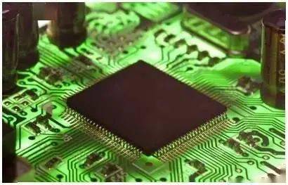
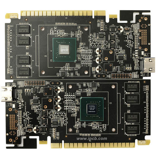
The internal components of smart phone front-end modules have increased dramatically, greatly limiting the available space. More than 60 filters have been installed in current high-end mobile phones, and it is foreseeable that there will be more than 100 filters in the next generation. Each filter is targeted at a specific radio frequency band and requires unique design and performance characteristics. Integrating such a large number of different components in a very limited space presents many challenges for design and manufacturing teams. For these reasons, the form factor, heat dissipation and performance improvement have become the key characteristics of the internal filter of the front-end module.
Market demand
So far, the signal selection of smartphones has mainly adopted two filtering techniques. Piezoelectric materials generate sound waves that can travel freely on the surface of the material (SAW: surface acoustic wave) or between active layers (BAW: bulk acoustic wave).
The current SAW filter is very suitable for the low and medium 4G frequency band, but it is difficult to meet the higher requirements of 5G (high TCF, low Q factor, low coupling coefficient) and frequency. Due to the high thermal expansion of its substrate (usually lithium tantalate or lithium niobate), the frequency response of the SAW filter is sensitive to temperature changes. In the last step of the device manufacturing process, adding an extra layer to the top of the metal layer can compensate for the temperature sensitivity problem to a certain extent, but at the same time the new layer will affect the coupling efficiency and final performance of the filter.

The BAW filter can maintain good performance at higher frequencies, but the size cannot be as thin as the SAW filter, which is a big challenge for module integration. In addition, its manufacturing process is more complicated, and the multiplexers and duplexers that can be integrated on the same chip are also limited.
Film POI
Since it is impossible to compromise on certain performance indicators, Soitec has developed a new type of substrate to help operators and mobile phone manufacturers meet the challenges in response to the more stringent requirements of new 5G network functions. The POI substrate consists of a thin layer of single crystal piezoelectric material (currently single crystal lithium tantalate) covering a silicon dioxide layer and a high resistivity substrate, as shown in Figure 1a. The thickness of the top layer of lithium tantalate is generally between 0.3 and 1 μm. This thin-film POI substrate is made using Soitec's Smart-Cut™ process, which ensures high uniformity of the board layer and high-quality mass production. This structure can guide the sound wave on the surface of the substrate and concentrate its energy in the thin layer of lithium tantalate on the top with minimal loss (Figure 1b). With this new type of substrate, filter designers can use substrate materials with better coupling coefficients (k2) and lower thermal expansion coefficients, thereby designing resonators with high quality factors at higher frequencies, low temperature sensitivity, and larger bandwidths. Filter. At the same time, multiple filters can be integrated on the same chip.
The POI substrate includes a piezoelectric material layer, a buried oxygen layer and a silicon layer. The piezoelectric thin layer with high uniformity limits the energy of guided waves and achieves high-performance acoustic characteristics. The buried oxygen layer only guides high-speed waves in a targeted manner and suppresses piezoelectric materials, thereby reducing thermal expansion and thus temperature sensitivity. This structure can achieve higher signal selectivity and frequency stability when temperature changes. Since filter component manufacturers no longer need to add a thick layer on the top to constrain the piezoelectric material, compared with TC-SAW, it also simplifies the manufacturing process and improves the coupling efficiency.
SAW filters using POI substrates can achieve extremely low insertion loss, enabling device manufacturers to effectively manage energy consumption. Compared with other solutions, the POI-based SAW filter has the advantages of high Q factor, high coupling to high bandwidth filters, extremely low TCF, and highly integrated filters on the same chip.
In addition, it is worth noting that the filter design based on the POI substrate is very similar to the technology required for the SAW filter design based on the bulk piezoelectric wafer; at the same time, the manufacturing process only requires a few simple steps (standard metal layer deposition is used for the main body) .
Design of SAW resonator and filter based on POI
We measured and characterized the actual performance of SAW resonators based on lithium tantalate wafers and thin-film POI, and the results showed the performance improvement of the POI substrate. In this experiment, a dipole single-port resonator is used, with a total of 120 interdigital pairs and 20 electrodes on each side to achieve mirror images. The acoustic aperture is set to 40 λ, the distance between the interdigital and the electrode is 1.2 μm, and the metal/spacing ratio is 0.5. The POI substrate used in the experiment has the following characteristics: 600nm thick (YX)/42°LiTaO3 layer connected with 500nm thick silicon dioxide layer connected with high resistivity silicon layer (100).
Coupling coefficient k2
The coupling coefficient k2 of POI can reach 8.13%, while the bulk LiTaO3 wafer of the traditional TC-SAW device is only 5.98% (see Figure 3). k2 is calculated from 1-fr2/fa2 (where fr is the resonant frequency and fa is the anti-resonant frequency). The high k2 of the POI substrate enables the design of a large bandwidth filter to cover some of the new 5G frequency bands (up to 6% bandwidth of the center frequency).
Resonance k2 measurement results for bulk and POI substrates.
Another significant improvement in the performance of the POI substrate is shown in the Bode Q factor during anti-resonance. Under the same conditions, the Q factor of the bulk LiTaO3 is 935, and the result of the POI substrate is 2200, so that the SAW filter can compete with the BAW filter in the L-band and C-band.