PCB process chip packaging technology detailed explanation
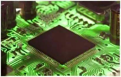
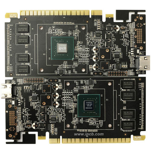
1.BGA (ball grid array) is also called CPAC (globe top pad array carrier). A display of spherical contacts, one of the surface mount packages.On the back of the printed circuit board,spherical bumps are produced in the display mode to replace the pins, and the LSI chip is assembled on the front side of the printed circuit board,and then sealed by molding resin or potting.Also known as bump display carrier (PAC).The pin can exceed 200, which is a package for multi-pin LSI.The package body can also be made smaller than QFP (Quad Flat Package).For example, a 360-pin BGA with a pin center distance of 1.5mm is only 31mm square,while a 304-pin QFP with a pin center distance of 0.5mm is 40mm square.And BGA does not have to worry about pin deformation like QFP.
This package was developed by Motorola Company of the United States, and was first adopted in portable phones and other devices, and then popularized in personal computers. Initially, the BGA pin (bump) center distance was 1.5mm, and the number of pins was 225. There are also some LSI manufacturers that are developing 500-pin BGAs. The problem with BGA is the visual inspection after reflow soldering. American Motorola Company refers to the package sealed with molded resin as OMPAC, while the package sealed with potting method is called GPAC.

2.C-(ceramic) represents the mark of ceramic package. For example, CDIP stands for ceramic DIP.It is a mark that is often used in practice.
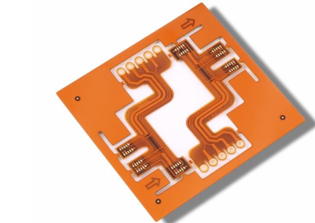
3.COB (chip on board) chip on board packaging is one of the bare chip mounting technologies.The semiconductor chip is handed over and mounted on the printed circuit board. The electrical connection between the chip and the substrate is realized by wire stitching and covered with resin to ensure reliability.Although COB is the simplest bare chip mounting technology, its packaging density is far inferior to TAB and flip-chip bonding technology.
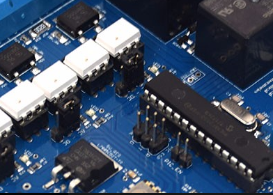
4.DIP (dual in-line package)
Dual in-line package. One of the plug-in packages, the pins are drawn from both sides of the package, and the package materials are plastic and ceramic. European semiconductor manufacturers mostly use DIL.
DIP is the most popular plug-in package, and its application range includes standard logic ICs, memory LSIs, and microcomputer circuits. The pin center distance is 2.54mm, and the number of pins is from 6 to 64. The package width is usually 15.2mm. Some packages with widths of 7.52mm and 10.16mm are called SK-DIP (skinny dual in-line package) and SL-DIP (slim dual in-line package) narrow-body DIP respectively. But in most cases, no distinction is made, and they are simply collectively referred to as DIP. In addition, ceramic DIP sealed with low-melting glass is also called Cerdip (see 4.2).
4.1DIC (dual in-line ceramic package) Another name for DIP (including glass seal) of ceramic package.
4.2Cerdip:Ceramic dual-in-line package sealed with glass, used for ECL RAM, DSP (digital signal processor) and other circuits. Cerdip with glass window is used for ultraviolet erasable EPROM and microcomputer circuit with EPROM inside. The pin center distance is 2.54mm, and the number of pins is from 8 to 42. In Japan, this package is expressed as DIP-G (G means glass seal).
4.3SDIP (shrink dual in-line package) Shrink DIP. One of the plug-in packages, the shape is the same as the DIP, but the pin center distance (1.778mm) is smaller than the DIP (2.54mm), so it is called this. The number of pins ranges from 14 to 90. There are two types of ceramics and plastics. Also known as SH-DIP (shrink dual in-line package)
5.flip-chip
Flip-soldering the chip.One of the bare chip packaging technologies is to make metal bumps in the electrode area of the LSI chip, and then connect the metal bumps to the electrode area on the printed substrate by pressure welding. The footprint of the package is basically the same as the chip size. It is the smallest and thinnest of all packaging technologies. However, if the thermal expansion coefficient of the substrate is different from that of the LSI chip, a reaction will occur at the joint, which will affect the reliability of the connection. Therefore, it is necessary to use resin to reinforce the LSI chip, and use a substrate material with substantially the same thermal expansion coefficient.
6.FP (flat package)
Flat package. One of surface mount packages. Another name for QFP or SOP (see QFP and SOP). Some semiconductor manufacturers use this name.
7.H-(with heat sink)
Indicates a mark with a radiator. For example, HSOP means SOP with heat sink.
8.MCM (multi-chip module)
Multi-chip components.A package in which multiple semiconductor bare chips are assembled on a wiring substrate.According to the substrate material, it can be divided into three categories: MCM-L, MCM-C and MCM-D. MCM-L is a component using a common glass epoxy multilayer printed circuit board.The wiring density is not very high and the cost is low. MCM-C uses thick film technology to form multilayer wiring, and uses ceramic (alumina or glass ceramic) as a substrate component,which is similar to a thick film hybrid IC using a multi-layer ceramic substrate. There is no obvious difference between the two. The wiring density is higher than MCM-L.MCM-D is the use of thin film technology to form multilayer wiring, with ceramic (aluminum oxide or aluminum nitride) or Si, Al as the substrate component. The wiring scheme is the highest among the three components,but the cost is also high.