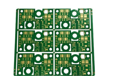
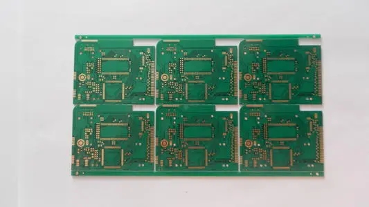
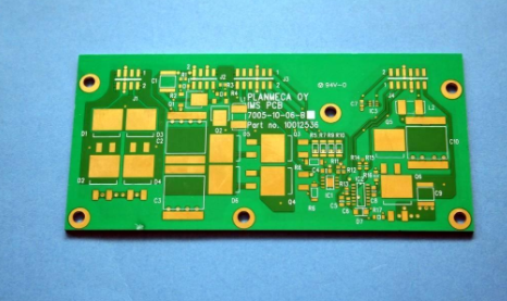
1. Determine the number of PCB layers
The size of the printed circuit board and the number of wiring layers need to be determined at the beginning of the design. If the design requires the use of high-density ball grid array (BGA) components, the small number of wiring layers required for the wiring of these devices must be considered. The number of wiring layers and stack-up mode will directly affect the wiring and impedance of printed lines. The size of the plate helps determine the layering pattern and the width of the printed line to achieve the desired design effect.

For years, it has been assumed that fewer layers mean lower costs, but there are many other factors that affect the cost of making a board. In recent years, the cost differential between multilayer panels has been greatly reduced. At the beginning of the design, more circuit layers were used and the copper coating was distributed evenly, so as to avoid having to add new layers only at the end of the design when a few signals did not conform to the defined rules and space requirements. Careful planning prior to design will reduce a lot of trouble in wiring.
2. Design rules and limitations
The automatic routing tool itself does not know what to do. To accomplish the wiring task, the wiring tool needs to work under the correct rules and constraints. Different signal cables have different wiring requirements. The signal cables with special requirements must be classified according to the design. Each signal class should have a priority, and the higher the priority, the stricter the rules. Rules related to printed line width, number of holes, parallelism, interaction between signal lines and layer limits, these rules have a great impact on the performance of wiring tools. Careful consideration of design requirements is an important step in successful wiring.
3. Component layout
For the assembly process, manufacturability design (DFM) rules impose restrictions on component layout. If the assembly department allows components to move, the circuit can be optimized to facilitate automatic wiring. The rules and constraints defined affect the layout design.
Routing channels and through-hole areas should be considered in layout. These paths and areas are obvious to the designer, but the automatic routing tool considers only one signal. By setting the routing constraints and setting the layer where the signal line can be laid, the routing tool can complete the routing as the designer intended.
How to achieve efficient automatic PCB routing
4. Fan out design
During the fan out design phase, to enable the automatic routing tool to connect component pins, each pin of the surface mount device should have at least one through-hole so that the board can be used for inner bonding, in-line testing (ICT), and circuit reprocessing when additional connections are required.
To make the automatic wiring tool efficient, it is important to use as many hole sizes and printed lines as po
ssible, with an interval of 50mil being ideal. Use a type of through-hole that gives the number of routing paths. On-line test of circuit should be considered when designing fan out. Test fixtures can be expensive and are usually ordered near full production, when it is too late to consider adding nodes to achieve 100% testability.
After careful consideration and prediction, the design of circuit on-line test can be carried out in the early design stage and later in the production process. The type of through-hole fan out can be determined based on the wiring path and circuit on-line test. Power supply and grounding also affect the wiring and fan out design. To reduce the filter capacitor impedance of cable, via should as far as possible near the surface-mount device pins, manual wiring can be used when necessary, it may affect the originally envisaged wiring path, even may cause you to reconsider using what kind of a hole, must therefore be considered the relationship between impedance and hole and pin set via the specifications of the priority.
5. Manual wiring and key signal processing
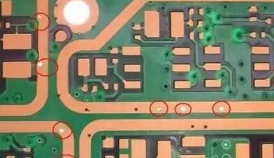
Although this paper focuses on automatic wiring, manual wiring is and will be an important process in PCB design. Manual routing is helpful for automatic routing tools. As shown in Figures 2A and 2b, the selected network (NET) can be manually routed and fixed to form a path that can be relied upon for automatic routing.
Regardless of the number of critical signals, wiring these signals first, manual wiring or combined with automatic wiring tools. Critical signals usually have to be carefully designed to achieve the desired performance. After wiring is completed, the signal wiring is checked by the relevant engineering personnel, which is a much easier process. After the check
is passed, the wires are fixed and automatic wiring of the remaining signals begins.
6. Automatic wiring
Wiring of key signals needs to consider controlling some electrical parameters during wiring, such as reducing distributed inductance and EMC, and wiring of other signals is similar. All EDA vendors provide a way to control these parameters. The quality of automatic wiring can be guaranteed to a certain extent by knowing what input parameters the automatic wiring tool has and how they affect wiring.
Common rules should be adopted for automatic routing of signals. By setting restrictions and no-wiring areas that limit the layers used for a given signal and the number of holes to be used, the wiring tool can automatically route the wires as designed by the engineer. If there is no limit to the number of layers used by the automatic routing tool and the number of holes laid, each layer will be used for automatic routing and many holes will be created.
After the constraints are set and the rules created are applied, automatic wiring will achieve a similar result to what is expected, although there may be some cleaning up to do, as well as securing space for other signals and network wiring. After a part of the design is completed, it is fixed to prevent the subsequent wiring process.
The same procedure is used to route the rest of the signals. The number of routes depends on the complexity of the circuit and how many general rules you define. After each class of signal is completed, constraints on the rest of the network routing are reduced. But with that comes a lot of signal wiring that requires manual intervention. Today's automatic routing tools are very powerful and can typically complete 100% wiring. However, when the automatic routing tool has not completed all signal routing, the remaining signals need to be manually routed.
7. The design points of automatic wiring include:
1) Slightly change the Settings and try out multiple routing paths;
2) Keep the basic rules unchanged, try different wiring layers, different printed line and spacing widths, different line widths, different types of holes such as blind hole, buried hole, etc., observe the influence of these factors on the design results;
3) Let the cabling tool process those default networks as needed;
4) The less important the signal, the more freedom the automatic routing tool has to route it.
8. Wiring arrangement
If you are using an EDA tool software that can list signal routing lengths, check this data and you may find that some signal routing lengths are very long with few constraints. This problem is relatively easy to handle, and manual editing can shorten the signal routing length and reduce the number of holes. During the cleaning process, you need to determine what wiring is right and what wiring is not right. Like manual routing designs, automatic routing designs can also be organized and edited during inspection.
9. Appearance of circuit board
Previous designs often focused on the visual effects of the circuit board, but that is no longer the case. The circuit board designed automatically is not as beautiful as manual design, but it can meet the requirements of electronic characteristics, and the integrity of the design is guaranteed.