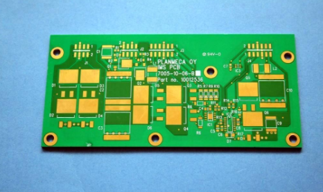
In smt printing, it often happens that the solder paste printing is cheap, the printing is missing, the thickness is too thick, etc.

Question: Can a small spatula be used to remove the misprinted solder paste from the PCB board? Will this get solder paste and small solder balls into holes and small gaps?
Answer: Using a small spatula to remove the solder paste from the misprinted board may cause some problems. It is generally feasible to immerse the misprinted board in a compatible solvent, such as water with some additives, and then use a soft brush to remove the small tin beads from the board. I would rather soak and scrub repeatedly than violently dry brushing or shoveling. After the solder paste is printed, the longer the operator waits to clean the misprint, the more difficult it is to remove the solder paste. Misprinted boards should be placed in the soaking solvent immediately after the problem is discovered, because the solder paste is easy to remove before it dries.
Avoid wiping with cloth strips to prevent solder paste and other contaminants from smearing on the surface of the board. After soaking, scouring with a gentle spray can often help remove unwanted tin drafts. It is also recommended to use hot air for drying. If a horizontal stencil cleaner is used, the side to be cleaned should face down to allow the solder paste to fall off the board.
As usual, paying attention to some details can eliminate undesirable situations, such as misprinting of solder paste and removal of cured solder paste from the board. It is our goal to deposit an appropriate amount of solder paste at the desired location. Dirty tools, dried solder paste, and misalignment of the template and the board may cause undesirable solder paste on the bottom surface of the template or even the assembly. During the printing process, the template is wiped according to a certain rule between printing cycles. Ensure that the template is located on the pad, not on the solder mask, to ensure a clean solder paste printing process. Online, real-time solder paste inspection and inspection before reflow after component placement are all process steps that help reduce process defects before soldering occurs.
For fine-pitch templates, if the thin template cross-section bending causes damage between the pins, it will cause solder paste to deposit between the pins, causing printing defects and/or short circuits. Low-viscosity solder paste may also cause printing defects. For example, the high operating temperature of the printer or the high squeegee speed can reduce the viscosity of the solder paste in use, and cause printing defects and bridging due to the deposition of too much solder paste.
In general, the lack of adequate control over materials, solder paste deposition methods and equipment are the main causes of defects in the reflow soldering process.
Question: What type of depaneling equipment for assembly panels provides good results?
Answer: At present, there are several sub-board systems that provide various techniques for sub-boarding assembly boards. As usual, many factors should be considered when choosing this type of equipment. Regardless of whether routing, sawing, or blanking is used to separate the individual boards from the composite board, stable support during the boarding process is an important factor. Without support, the resulting stress may damage the substrate and solder joints. Distorting the board, or stressing the assembly during board splitting, can cause hidden or obvious defects. Although sawing can often provide small gaps, cutting or punching with tools can provide cleaner, more controlled results.
In order to avoid component damage, many assemblers try to keep the component solder joints at least 5.08mm away from the edge of the board when it is required to separate the board. Sensitive ceramic capacitors or diodes may require extra care and consideration.
The above is the introduction of how to remove misprinted solder paste in SMT printing. Ipcb also provides PCB manufacturers and PCB manufacturing technology.