Circuit board factory: What are the defects of Protel99?
PCB working layer type
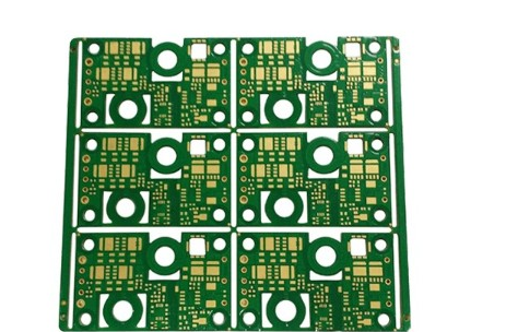
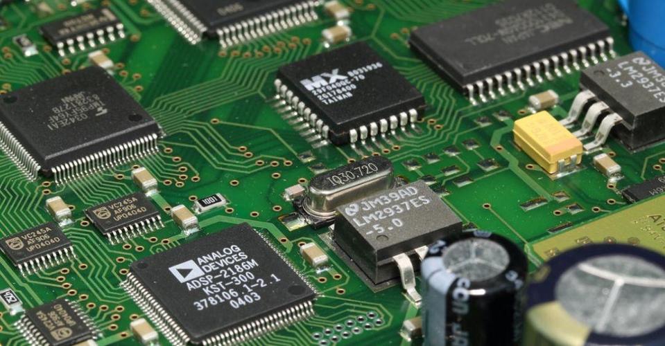
Before we proceed with the PCBA board design, the first step is to select the applicable working layer. Protel 99 SE provides many types of working layers. Only after understanding the functions of these working layers, can the printed circuit board be designed accurately and reliably.
The working layers provided by Protel 99 SE can be roughly divided into 7 categories: Signal Layers (signal layer), InternalPlanes (internal power/ground layer), Mechanical Layers (mechanical layer), Masks (solder mask), Silkscreen (silk screen), Others (other working level) and System (system working layer), execute the menu command [Design] design/[Options...] option in PCB design, you can set the visibility of each working layer.

1.Signal Layers
Protel 99 SE provides 32 signal layers, including [TopLayer] (top layer), [BottomLayer] (bottom layer), [MidLayer1] (middle layer 1), [MidLayer2] (middle layer 2)...[Mid Layer30] (middle layer) Layer 30). The signal layer is mainly used to place components (top and bottom) and traces. The signal layer is positive, that is, the traces or other objects placed on these working layers are copper-clad areas.
2.InternalPlanes (internal power supply/ground plane)
Protel 99 SE provides 16 internal power/ground planes (referred to as internal electric planes): [InternalPlane1]-[InternalPlane16]. These working levels are dedicated to laying out power and ground wires. The traces or other objects placed on these layers are copper-free areas, that is, these working layers are negative. Each internal power/ground layer can be given an electrical network name, and the printed circuit board editor will automatically connect this layer to other pads with the same network name (ie electrical connection) in the form of a pre-pull wire . In Protel 99 SE. It is also allowed to divide the internal power/ground layer into multiple sub-layers, that is, each internal power/ground layer can have two or more power supplies, such as +5V and +15V, and so on.
3.Mechanical Layers
There can be 16 mechanical layers in Protel 99 SE: [Mechanical1]-[Mechanical16]. The mechanical layer is generally used to place indicative information about board manufacturing and assembly methods, such as circuit board physical size lines, size marks, data materials, and Hole information, assembly instructions and other information.
4. Masks (solder mask, solder paste protective layer)
In Protel 99 SE, there are 2 solder masks: [Top Solder] (top solder mask) and (Bottom Solder] (bottom solder mask). The solder mask is negative, the solder placed on this layer Disks or other objects are copper-free areas. Usually in order to meet the requirements of manufacturing tolerances, manufacturers often require to specify a solder mask expansion rule to enlarge the solder mask. For different requirements of different pads, in the solder mask Multiple rules can be set. Protel 99 SE also provides 2 solder paste protective layers, namely [Top Paste] and (Bottom Paste). The solder paste protective layer and The role of the solder mask is similar, but when the "hot re-follow" (thermal convection) technology is used to install SMD components, the solder paste protection layer is mainly used to establish the silk screen of the solder mask. This layer is also negative. Similar to the solder layer, we can also enlarge or reduce the solder paste protection layer by specifying an expansion rule. For different requirements of different pads, multiple rules can also be set in the solder paste protection layer.
5.Silkscreen (silk screen layer)
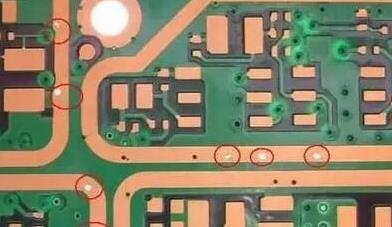
Protel 99 SE provides 2 silk screen layers, [Top Overlay] and [Bottom Overlay]. The silk screen layer is mainly used to draw the outline of the component, the number of the placed component or other text information. When placing PCB library components on the printed circuit board, the number and outline of the component will be automatically placed on the silk screen layer.
6.Others (other working levels)
In Protel 99 SE, in addition to the above-mentioned working layers, there are the following working layers: [KeepOutLayer] (forbidden wiring layer) The forbidden wiring layer is used to define the area where components are placed. Usually, we place a track or arc on the forbidden routing layer to form a closed area, in which automatic layout and automatic routing of components are allowed.
Note: If you want to auto-layout or auto-route some or all circuits, you need to define at least one forbidden wiring area on the forbidden wiring layer. [Multi layer] (Multilayer) This layer represents all signal layers, and the components placed on it will be automatically placed on all signal layers, so we can use [MultiLayer] to add pads or penetrating vias Quickly place it on all signal layers.