1.Formation and response of voids
Although the fr4 pcb solder paste is composed of 88-90% solder alloy ball by weight and 10-12% organic auxiliary materials,the volume ratio of the two evenly mixed is half.Therefore,when the solder joint is healed in strong heat and becomes the main body of the solder joint,the organics with light weight will be squeezed out of the main body of the alloy under normal circumstances, and will be separated from the solder joint.However,once the surface of the solder joint has solidified,so that the internal organic matter cannot escape to the outside in time, it is bound to be cracked into gas and stay in the solder joint,forming ubiquitous gas holes or voids.Unfortunately,once the solder paste absorbs water,the situation will be worse. Basically, the void formed by gas expansion is spherical.This kind of back-welding void is not only much more than that of wave welding in quantity or volume,but also has different causes and should not be confused.

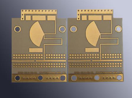
2.Holes in BGA pad
The voids in various lead free solder paste solder joints are the most and the largest in BGA or CSP ball pin solder joints. One reason is that when the upstream packaging plant planted the ball on the bottom of the BGA carrier plate,it temporarily attached the welding paste (G1ue FluX),and then it was fused by hot air,which may have formed a hole in the ball.Of course,there will be more holes in the solder paste after soldering back in the assembly plant. Most of them are the result of the gas in the solder paste rising and drilling into the sphere,and the two phases flow together to help the situation.This kind of hole that BGA ball foot cannot avoid has been accepted by international norms in fact. Since the prevalence of HDI interconnection technology (referring to both the layer-increasing method and the laser micro-blind hole),the interconnection between BGA or CSP and the inner layer does not need to pass through PTH, but only through the micro-blind hole with local conduction. This will not only reduce the irrelevant drilling of other layers (such as ground layer or power layer), but also improve the quality of signal integrity; In addition, the noise can be reduced by shortening the signal line, making the high-speed signal work more perfect. However, once the ball pad in the BGA area of the board is equipped with a small blind hole (Viain Pad), the solder paste back-welding will inevitably cause a blow void at the ball foot, which will greatly affect the strength of the solder joint. Fortunately, at this time in 2006, with the rapid progress of copper electroplating technology, not only the large and small blind holes can be filled with copper, but also the small diameter PTH can be filled. Therefore, circuit board manufacturers with good technology should not continue to have the problem of blind hole blowing on the solder joint. At present, in the transition period, when BGA in stock is still a ball pin with lead 63/37, but the solder paste used for assembly is lead-free SAC, the former will melt into liquid first, and the latter with higher mp will rise into the liquid ball pin if any gas hole occurs during welding, and its floating path is much easier than escaping from the ball. In addition, once the printed solder paste has been hygroscopic, it is not surprising that the adjacent pins are competing to make a super large hole with short circuit. In principle, if there are more than one BGA on the board, a long saddle type reflux curve should be used to drive away the volatiles and reduce the blowhole(solder blow hole).
3.Voids from surface treatment
In some PCBA surface treatment films, those with high organic content (I-Ag and OSP are the most typical) are also easy to crack into small holes in the subsequent strong heat. Its characteristic is that most of them only stay at the interface. Although the number is large,the volume is not large. It is called "interface microhole". This kind of continuous film micro-hole, whether wave welding or back-welding, often occurs, and silver immersion is more serious.The solution is to improve the formula and process of surface treatment. The silver-dipped layer is easy to tarnish when it encounters a small amount of sulfur gas in the air. In order to prevent tarnish and prevent the rapid migration of silver metal (Leaching) and even damage the insulation, a thin layer of organic protective film is deliberately formed on the surface of the silver-dipped layer to block such defects. However, in the welding reaction, silver metal will rapidly dissolve into liquid solder (dissolution rate 43.6μ In/sec), and expose the bottom copper to make it and molten tin rapidly form Cu6Sn5 and weld it firmly. Unfortunately, the organic film could not leave in time, so it had to remain at the original interface for cracking and gas generation.It is also called champagne foam because it occurs comprehensively. As for the performance of the new generation OSP, it has also been improved in terms of the compactness of its film,even if 0.3μ The film thickness of m can still protect the bottom copper from oxidation and rust in strong heat. Therefore, if the OSP film in wave welding or reflow welding can be driven away by the flux in time,the growth of Cu6Sn5 can be completed and welded firmly. Once the OSP membrane is not driven out in time, it will be cracked by strong heat and gas will form holes. A good OSP film should not only be heat-resistant, but also not too thick to prevent cracking and gas generation when it is tenacious in welding. However, if nitrogen is used in the reflow furnace,this dilemma will be greatly improved.
4.Tin powder and flux are oxidized and gassed to form holes
When some large plates are reflowed,the heat absorption section (Soak) of the reflow curve must be extended (for example, more than 90 seconds), so that the peak temperature can be sprinted after the plates to be welded are full of heat energy inside and outside. In this kind of slow rising strong heat of 150-180 ℃ and the long time of double boiling above the subsequent melting point, not only the tin powder will be oxidized, but sometimes even the flux will be oxidized and deteriorated. At this time, the holes in all solder joints will inevitably increase. Once the surface of the small tin ball is too oxidized to heal, it will have to be pushed out and cause other problems. Although it is a positive solution to choose flux with good oxidation resistance, it is not easy. The more practical approach is to use nitrogen environment for back-welding, which will immediately reduce such problems as cavities and poor tin eating.
5.The solder pad on the surface of the PCB board rejects tin and forms voids
There are five to six types of solderability surface treatment for PCB copper pad.Once the pad surface has already presented solder rejection, the solder paste has been printed on the pad surface in full, but when the pure tin and local bad base (copper or nickel) cannot form IMC during strong heat healing, the solder paste distributed there will be snatched away by the neighbors with good tin on the left and right,so as to form a vacuum instantaneously.At this time,half of the volume of organic matter in the solder paste will not escape to the outside world, but will be attracted by the local vacuum nearby, and then quickly gather gas to blow into a large hole.Some BGA ball pads are treated by tin spraying.Once the tin surface is uneven and severely shrunk, large holes are likely to occur at the solder reject after the subsequent solder paste passes through the furnace. However,the large holes formed by the poor treatment of the PCB pad surface mostly occur in the BGA ball pin with a wide stage,and rarely in other narrow solder joints such as QFP.
6.The solder paste absorbs water to form a large hole
The holes blown by the failure of the organic matter to escape are not too large.However,once used,or placed for a long time after printing the paste and inhaled water, the holes blown by the organic matter will be very large, and even the three-dimensional space of the adjacent ball feet will be blown and squeezed into a short circuit. Such added moisture is lead and lead-free. There is no other good way to improve it.Generally,as long as the solder paste is placed in 90% RH for 20 minutes,it will absorb a large amount of water and blow into a large hole, which may even cause the spatter of molten tin and lead to additional tin spots on the fingers.We know that the site of solder paste printing must be kept low temperature and dry.
7.Hole from BGA upstream package
BGA does not use solder paste from the assembly plant to plant balls at the belly bottom in the packaging plant. For the sake of better coplanarity of many ball feet, it can only use soldering paste for the dual purposes of positioning and soldering.However,in the process of completing the ball planting in the reflow furnace,the solder paste welding principle is exactly the same, and the ball planting will also have holes. Therefore,during the feeding inspection, it is necessary to check whether there is any hole in the X-ray fluoroscopy with the abdomen facing up, so as to avoid unnecessary disputes between each other when "it is easy to break the head and difficult to break the foot" occurs afterwards on the fr4 pcb.