1. Simulated back welding
Generally, the downstream PCBA assembly process has about five heating experiences, namely:
(1) Solder paste and dispensing are printed on the front and hot-air soldering is performed.
(2) The reverse side is turned over and then solder paste is welded back.
(3) The pin parts shall be wave welded.
(4) It may undergo 1-2 times of rework and repair welding.
Therefore, most of the assembly manufacturers require that the empty plates of fr4 plate manufacturers also simulate more than five times of reflow according to the specific reflow curve, as a reference standard for whether they can withstand strong heat. In fact, even if the blank multilayer plate can pass the test of five times of simulated back-welding, it is difficult to ensure the safety of the assembler in the back-welding operation, and there will still be some rate of bursting in the actual installation. The main reason is due to the additional stress of components on the board.

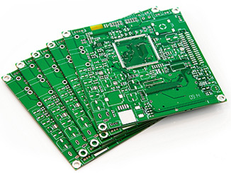
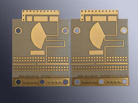
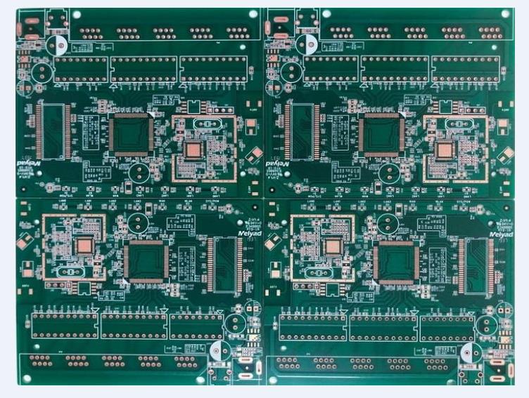
fr4 plate
The upwind of the hot-air back-welding furnace is usually about 50-60 ℃ higher than the downwind of the plate. The purpose of the downwind is to maintain the basic heat of the plate, and it is not necessary to maintain the same heat with the upwind at all, so as to avoid unnecessary energy waste and damage to the plate. In addition, when the reverse side is welded for the second time, it can also reduce the strong heat injury to the person who has been welded on the first side and the possibility of falling parts. However, these differences in heat of the upper and lower plates will inevitably lead to the difference in thermal expansion of both sides of the fr4 plate, and the slight humped arc bulge of the plate surface will occur during the back welding, which will lead to the tensile stress between the compact assembly and the fr 4 pcb. In particular, the huge heat obtained by integrating the reflow temperature and time has not only far exceeded the Tg of the plate, but also made the plate from lower than Tg α- 1 Glass state, transition to more than Tg α- The soft rubber state of 2. At this time, once there is a lot of local stress, it will cause blistering and bursting from the surface of the thick multilayer plate.
2. The weakness of the rubber knee of the plate
When the board is equipped with several large BGA or QFN front temples, the thermal expansion rate (CTE) of the chips (chips) inside the board is only 3-4 ppm/℃, which will force the thermal expansion rate of X and Y axes to 15 ppm/℃. The carrier plate of has to be pulled up and warped during back welding. The upward warping of these carrier plates and the downward bending of the fr4 pcb motherboard will inevitably damage the solder joint and the expanded plate if they are pulled against each other. There was an unwritten heating principle for plates, that is, the resin would double the energy of reaction when the temperature was raised by 10 ℃, and the volume and mass were the largest in the process of hot-air reflow? The degree of heating is also much higher than that of various components on the board. In fact, FR-4 plate is below Tg α In the glass state, the CTE of the Z axis is up to 55-60 ppm/℃, which is far more than 14-15 pm/℃ in the X and Y
directions clamped by the glass fiber cloth. Once in α 2. In the rubber state, the CTE of its Z axis is higher than 250pm/℃, and any local uneven stress on the plate surface may cause blistering or bursting of the outer layer.
3. Location and cause of easily exploded plate
(1) Large copper surface area of inner layer
Because the thermal expansion coefficient (CTE) of copper (CTE is only 17pm/℃) and resin Z direction is too far away, the large copper surface area is easy to explode in strong heat (referring to the integration of temperature and time). The solution is to deliberately arrange a few non-functional through-holes in the large copper area as rivets, which can not only help heat dissipation but also reduce the explosion disaster of multi-layer thick plates. However, the previous question is that the quality of PTH hole copper must be good enough, and its elongation should be controlled above 20% to make sense. In fact, due to the great progress in the current copper plating process, the excellent liquid medicine suppliers have already exceeded 30% in the copper plating layer elongation, which is not difficult. The result of the latest negotiation between the current backplate manufacturer and downstream customers is tentatively set at 18% as the lower limit of the manufacturing process. In the future, under the pressure of the prevalence of lead-free soldering, it will rise to the minimum specification of 20% sooner or later. Having said that, however, there are still many second-line and third-line copper plating process suppliers, whose quality is far behind the current requirements for thick plates by 18%, and even less than the 15% required for general multilayer plates. Of course, the management of the on-site copper plating bath and the inspection of the hole copper quality of the fr4 pcb should not be sloppy, to reduce the expansion and cracking of the plate in the lead-free reflow. In the event of plate bursting in the large copper surface area, many people intuitively react that the inner black brown film is poor and the adhesion is insufficient. However, when the micro-section is exquisitely made, and the crack has been filled with glue twice and further finely ground in the crack, it can be clear whether the crack is caused by the blackening layer of the copper foil. There is no need to waste words at all.
(2) Through-hole dense area
For example, if the ball pad and the many dense through-holes connected with the inner layer of the belly bottom of the large BGA are not blocked before the back-welding, a large amount of heat energy from the downwind will enter into the air, causing the heat from the upper and lower parts to be added and difficult to dissipate. Of course, it is easy to cause local plate explosion during the double suffering, and even the welding point of the ball foot will also overheat. In addition, when the plate is turned over for secondary re-welding, it may also cause the remelting or strength reduction of the previous solder joint. As for multi-pin connectors, whether using traditional wave welding or PIH solder paste back-welding, it will bring extra stress and easy to burst, which is also a very difficult problem. However, when the finished board wants to block these holes with green paint to isolate the hot air, it can be said that the project is arduous and difficult, and no one can be sure that it is completely filled without flaws. As for those who use special resin with good quality as filler, the cost is too expensive for general circuit board manufacturers. It is difficult to prevent the penetration of liquid medicine in the wet surface treatment of the subsequent welding pad of the through hole that is not firmly blocked. Even in the process of tin spraying, the tin slag may be squeezed into and form hidden troubles. Any defect in the fr4 pcb process will cause subsequent fatal injury. As for the multi-pin insertion area of the connector, although it is also a porous and dense hole zone, because the Thai half adopts the wave welding or selective welding with a single side short and strong heat (the strong heat time is only 4-5 seconds), its disaster and pain are far less than the dread of hot air reflow "lasting for 90 seconds above the melting point". Moreover, the part script body can also assist in heat absorption and heat dissipation, so the probability of plate bursting can also be reduced.
(3) Local blistering of outer layer
Multi-layer plates have already jumped out of the one-time traditional pressing method. Whether it is the use of RCC or film lamination, or the non-HDI progressive pressing of high-order multilayer plates, the heating rate and heat of the outer layer in the back-welding must be much higher than the inner core plate. Therefore, once the back-welding furnace of the downstream assembler is not ideal, or its back-welding curve still continues the old and improper lead-containing practice, or even has no knowledge of the new concept of lead-free back-welding, such as slow heating, long heat absorption, and flat peak temperature, it will inevitably become a considerable number of wronged bursting plates due to the ignorance of the assembler. Generally, the fr4 plate manufacturers have less in-depth understanding of the downstream back-welding principle, while the assembly industry generally knows too little about the dread of lead-free back-welding, and has always stood in the buyer's position with a strong attitude. Once the plate is exploded, the fr4 pcb factory must be blamed. Therefore, the scenes of no mistake and no mistake in the land cutting indemnity continued to be staged! Most of these local outer blisters are near the large BGA or QFN, especially the low and legless QFN, which is the most prone to problems. As for the buried hole ring of the inner PTH, has it undergone good black oxidation treatment before the outer layer is pressed? Even if it has been done, but the area of the hole ring is too small, and the grip is not enough, can it be successfully broken through? This is also the problem. Other areas with dense through-holes such as edges and corners of plates are also high-risk areas, and the probability of problems when the heat is too large is not small.
(4) Multiple plate bursts due to repeated strong heat
Lead-free soldering of fr4 pcb will continue the previous practice, mainly by double-sided SMT solder paste reflow, plus a transmission wave soldering or partial selective surge soldering. If the solder pad surface treatment of fr4 pcb is lead-free tin spraying, it means another wave soldering. Under the torture of 3-4 times of intense heat, the multilayer board has already been in danger. Once the plate is placed for too long, resulting in the accumulation of stress energy, or if it is not baked after pressing to eliminate the stress, the CTE differences between the plate members (glass fiber, resin, copper layer) and other members will gradually emerge and the stress release behavior will occur, or when the finished plate has inhaled water, it will be even worse; Once you get the chance to relax and vaporize due to intense heat, of course, you will reveal your nature and cause instant damage to the binding force. At this moment, if proper baking can be performed before reflow, the occurrence of plate bursting can be reduced. If there is other strong heat after the above three conventional welding, such as repair welding by back-welding or wave welding, or rework repair welding by replacing the active component, it may cause plate explosion, and the operator cannot handle it carelessly. According to the long-term experience of the production line, the damage of lead-free reflow to multi-layer plates is about 2-3 times more than that of lead-free wave soldering. Therefore, once some local welding defects are found, manual soldering should be used as far as possible to replace the reflow and wave soldering that were originally put online again in a big action on the fr4 pcb.