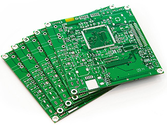
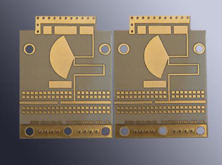
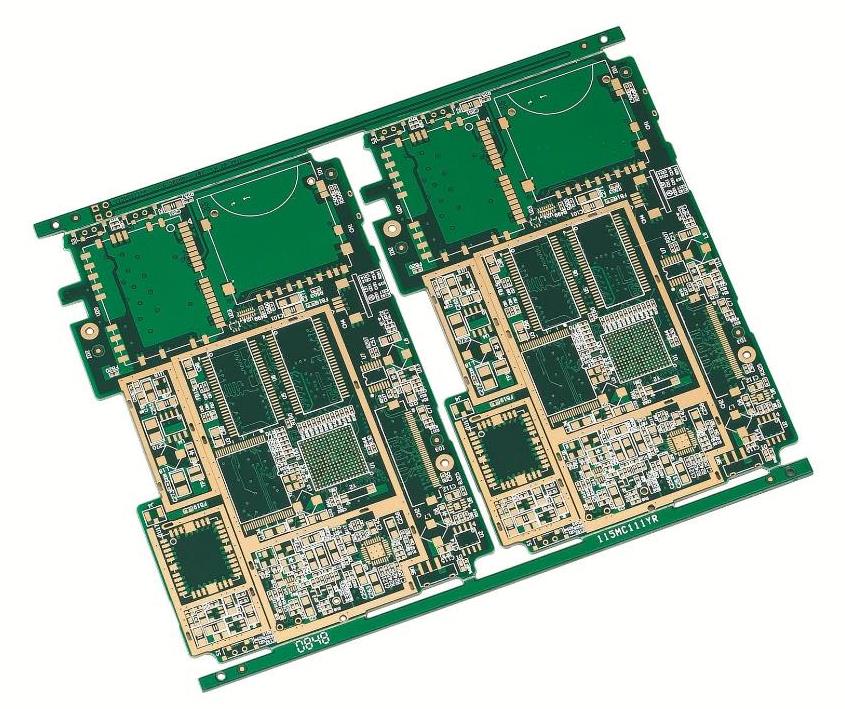
1. Green paint construction
The ball pad at the bottom of the BGA of fr4 pcb is welded in the way of "green paint limit". Once the green paint is too thick (more than 1mil) and the cushion surface is too small, there will be a "crater effect" that is difficult for wave welding to enter. In addition, under the attack of a large amount of flux and high heat, the ball planting operation of the cutting board will force the solder to penetrate into the bottom of the green paint edge, which will cause the green paint to float away. This is quite different from the solder paste welding of PCB processing pad. Generally, if the SMD copper pad of such carrier plate is slightly larger (sometimes including nickel and gold), the green paint can climb up to the circumference of 4mil. Since tin cannot flow to the outer straight wall of the copper pad, its strength is not as strong as the NSMD solder joint formed by all copper pads under stress. The stress of SMD solder joint is not easy to dissipate, so its "fatigue life" is generally only 70% of NSMD. In fact, the designers and producers of general packaging carrier boards do not know much about this logic, which makes the strength of various BGA bearing pads on mobile phone circuit boards increasingly unsafe in the future lead-free soldering.

1) Green paint plug hole
Generally, the function of the green paint plug hole of the fr4 pcb is to facilitate the vacuum pumping and fast fixing of the board surface when the circuit board is tested; The second is to protect the line or solder pad near the through-hole on the first side from being infringed by the tin surge in the second side wave welding. However, if the filling is not firm and broken, it will still suffer from the endless aftereffects caused by tin spraying or wave welding.
2) Re-wave welding after fusion welding
After the fusion welding of some parts is completed on both sides, it is often necessary to insert and weld some components. As a result, the through-hole adjacent to the ball pad will also transfer the wave welding heat to the first side. As a result, the ball foot that has been welded by Reflow at the bottom of the belly may suffer from remelting again, and even may form unexpected cold welding or open circuit. At this time, temporary heat shield and wave shield can be used to insulate the upper and lower sides of BGA area.
3) Construction of hole plugging
The construction methods of green paint hole plugging of fr4 pcb include: dry film cover hole and printing flooding hole. It refers to the hole plugging on both sides of the printing board by passing through the hole. It refers to the hole plugging on the front and back sides, but the residual air will sometimes burst out in high temperature. Professional plugging is to use special resin to deliberately plug and cure the hole first, and then print green paint on both sides. No matter what method, it is difficult to perfect. For OSP boards, it is not feasible to plug in front or back with green paint, and there are many cases of tragic failure in the downstream. Because when OSP is done after the front stopper, it is easy to leave liquid medicine in the slit and hurt the pore copper, and the baking of the rear stopper will be detrimental to the OSP film, which is really a dilemma.
2. Installation of BGA
1) Printing of solder paste
The opening of the steel plate used should preferably be a trapezoidal opening with narrow top and wide bottom, so as to facilitate stepping on the foot and lifting the steel plate after printing without disturbing the solder paste. The metal part of the commonly used solder paste accounts for about 90%, and the size of the tin particles should not exceed 24% of the opening to avoid the blurring of the printing paste edge. The most commonly used BGA assembly paste is particle size 53 μ m. For CSP, the common particle size is 38 μ m。 For large BGA with a foot distance of 1.0-1.5mm, the thickness of its printed steel plate should be 0.15-0.18mm, and the thickness of its steel plate should be reduced to 0.1-0.15mm if it is less than 0.8mm. The "width to depth ratio" of the opening must be kept at about 1.5 to facilitate paste removal. At the corner of the opening of the square cushion of the closely spaced ones, an arc must be presented to reduce the seizure of tin particles. Once the width-depth ratio of the steel plate of the small-piece close-spaced round pad is less than 66%, the printing paste applied must be 2-3 mil larger than the pad surface, so that the temporary adhesion before fusion welding is better.
2) Hot-air fusion welding
After 90 years, forced convection hot air has become the mainstream of Reflow. The more heating sections in its production line, not only is it easy to adjust the "temperature time curve", but also the production rate will be accelerated. The current lead-free solders must have more than 10 sections on average to facilitate heating (up to 14 sections). When the high temperature in the profile has exceeded the Tg of the plate and has been together for too long, not only will the circuit board become soft, but also the expansion will cause the plate to burst, resulting in the inner line or PTH fracture and other disasters. The flux in the solder paste must be above 130 ℃ to show its activity, and its activity time can be maintained for 90-120 seconds. The average heat resistance limit of various components in the fr4 pcb is 220 ℃ and cannot exceed 60 seconds.