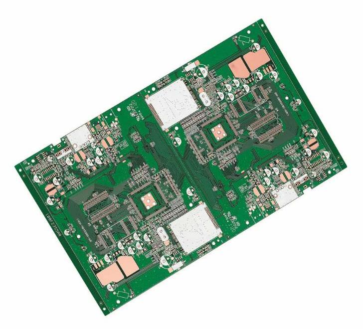
The basic design process of the general
PCB board is as follows
1. Preliminary preparation
This includes preparing component libraries and schematics. "If you want to do a good job, you must first sharpen your tools." To make a good board, in addition to designing the principles, you must also draw well. Before designing the PCB board, first prepare the component library of the schematic diagram SCH and the component library of the PCB board. The component library can use the library that comes with protel, but it is generally difficult to find a suitable one. It is better to make a component library yourself according to the standard size data of the selected device. In principle, make the component library of the PCB board first, and then make the component library of the SCH. The component library of the PCB board has high requirements, which directly affects the installation of the board; the component library requirements of the SCH are relatively loose, as long as you pay attention to defining the pin attributes and the corresponding relationship with the PCB board components. PS: Note the hidden pins in the standard library. After that is the design of the schematic diagram, and after it is done, it is ready to start the PCB board design.
2. PCB board structure design
In this step, according to the determined circuit board size and various mechanical positioning, draw the PCB board surface in the PCB board design environment, and place the required connectors, buttons/switches, screw holes, assembly holes, etc. according to the positioning requirements. And fully consider and determine the wiring area and non-wiring area (such as how much area around the screw hole belongs to the non-wiring area).
3. PCB board layout
The layout put it bluntly is to put the device on the board. At this time, if the preparations mentioned above are done, you can generate a netlist (Design-Create Netlist) on the schematic diagram, and then import the netlist (Design-Load Nets) on the PCB board diagram. I saw that the devices were all piled up, and there were flying wires between the pins to indicate the connection. The device can then be placed. The general layout is carried out according to the following principles:
1) According to the reasonable division of electrical performance, it is generally divided into: digital circuit area (that is, afraid of interference and interference), analog circuit area (afraid of interference), and power drive area (interference source);
2) The circuit that completes the same function should be placed as close as possible, and the components should be adjusted to ensure that the connection is simple; at the same time, the relative position of each functional block should be adjusted to make the connection between the functional blocks simple;
3) For components with large mass, the installation position and installation strength should be considered; heating elements should be placed separately from temperature-sensitive components, and thermal convection measures should be considered if necessary;
4) The I/O drive device should be as close as possible to the edge of the printed board and the lead-out connector;
5) The clock generator (such as crystal oscillator or clock oscillator) should be as close as possible to the device that uses the clock;
6) A decoupling capacitor (usually a monolithic capacitor with good high-frequency performance) needs to be added between the power input pin of each integrated circuit and the ground; when the circuit board space is dense, it can also be placed around several integrated circuits Add a tantalum capacitor.
7) A discharge diode should be added to the relay coil (1N4148);
8) The layout requirements should be balanced, dense and orderly, and should not be top-heavy or heavy. When placing components, the actual size of the components (occupied area and height) and the relative position between components must be considered. To ensure the electrical performance of the circuit board and the feasibility and convenience of production and installation, the placement of the devices should be appropriately modified on the premise that the above principles can be reflected to make them neat and beautiful. For example, the same devices should be placed neatly and oriented. Consistent, not "patched". This step is related to the overall image of the board and the difficulty of wiring in the next step, so it takes a lot of effort to consider. When laying out, you can make preliminary wiring for the places that are not sure, and fully consider them.
4. Wiring
Wiring is an important process in the entire PCB board design. This will directly affect the performance of the PCB board. In the design process of the PCB board, there are generally three divisions of wiring: the first is the wiring layout, which is the basic requirement for PCB board design. If the lines are not laid out, and there are flying wires everywhere, it will be an unqualified board, and it can be said that it has not yet started. The second is the satisfaction of electrical performance. This is a measure of whether a printed circuit board is qualified. This is after routing, carefully adjusting the wiring so that it can achieve the best electrical performance. Next is beauty. If your wiring is connected, there is nothing to affect the performance of the electrical appliance, but at first glance, it looks messy, colorful and colorful, then no matter how good your electrical performance is, it is still a piece of garbage in the eyes of others. This brings great inconvenience to testing and maintenance. The wiring should be neat and uniform, and not criss-cross without any rules. All of these must be realized under the condition of ensuring the performance of the electrical appliance and meeting other individual requirements, otherwise it will be abandoned. The wiring is mainly carried out according to the following principles:
1) In general, the power line and ground line should be wired first to ensure the electrical performance of the circuit board. To the extent permitted, try to widen the width of the power and ground wires, preferably the ground wire is wider than the power wire, and their relationship is: ground wire > power wire > signal wire, usually the signal wire width is: 0.2-0.3mm, The thin width can reach 0.05-0.07mm, and the power cord is generally 1.2-2.5mm. For the PCB board of the digital circuit, a wide ground wire can be used to form a loop, that is, a ground network can be used (the ground of the analog circuit cannot be used in this way).
2) Wire the lines with strict requirements (such as high-frequency lines) in advance, and avoid the adjacent parallel lines between the input end and the output end to avoid reflection interference. If necessary, ground wire isolation should be added, and the wiring of two adjacent layers should be perpendicular to each other, and parasitic coupling will easily occur in parallel.
3) The oscillator shell is grounded, the clock line should be as short as possible, and it should not be drawn everywhere. Below the clock oscillation circuit, the special high-speed logic circuit part should increase the area of the ground, and other signal lines should not be used to make the surrounding electric field approach zero;
4) Use 45-degree folded lines as much as possible, and do not use 90-degree folded lines to reduce the radiation of high-frequency signals; (double arcs should also be used for lines with high requirements)
5) Do not form a loop in any signal line. If it is unavoidable, the loop should be as small as possible; the vias of the signal line should be as few as possible;
6) The key lines should be as short and thick as possible, and protective ground should be added on both sides.
7) When transmitting sensitive signals and noise field signals through flat cables, use the method of "ground wire-signal-ground wire".
8) Test points should be reserved for key signals to facilitate production and maintenance testing
9) After the schematic wiring is completed, the wiring should be optimized; at the same time, after the preliminary network inspection and DRC inspection are correct, the unwiring area is filled with ground wires, and a large area of copper layer is used for ground wires. The places that are not used are connected to the ground as a ground wire. Or make a multi-layer
PCB board, power supply, ground wire each occupy one layer.