When designing
PCB board, we usually rely on previous experience and tips that we would normally find online. Every PCB board design can be optimized for a specific application, and usually, its design rules apply only to the target application. For example, analog-to-digital converter PCB board rules do not apply to RF PCB boards and vice versa. However, certain guidelines can be considered general to any PCB board design. Here, in this tutorial, we'll cover some basic questions and tips that can dramatically improve your PCB board design.
Power and Signal Distribution
Power distribution is a critical element in any electrical design. All your components rely on strength to perform their functions. Depending on your design, some components may have good power connections and some components on the same board may have poor power connections. For example, if all components are powered by one trace, each component will observe a different impedance, resulting in multiple ground references. For example, if you have two ADC circuits, one at the beginning and one at the end, and both ADCs read an external voltage, each analog circuit will read a different potential relative to themselves. We can summarize the power distribution in 3 possible ways: single point source, star source and multipoint source.
1) Single point power supply: The power and ground wires of each component are separated from each other. The power traces of all components meet only at a single reference point. A single point is considered suitable for power. However, for complex or large/medium sized projects this is not feasible.
2) Xingyuan: Xingyuan can be regarded as an improvement of a single point source. It differs due to its key characteristic: the same length of traces between components. Star connections are often used for complex high-speed signal boards with various clocks. In high-speed signal PCB boards, the signal usually comes from the edge and then reaches the center. All signals can travel from the center to any area of the board with a delay between areas.
3) Multi-point source: considered poor in any case. However, it is easy to use in any circuit. Multiple point sources can create reference differences between components and in common impedance coupling. This design style also allows high switching ICs, clocks and RF circuits to introduce noise in nearby circuits that share connections. Of course, in our daily life, we will not always be able to have a single type of distribution. The compromise we can achieve is to mix single-point sources with multi-point sources. You can have analog sensitive equipment and high speed/RF systems in one spot, while all other less sensitive peripherals in one spot.
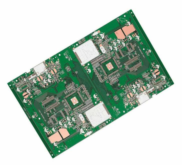
Powered aircraft
Have you ever wondered if you should use a power plane? The answer is yes. Power strips are one of the ways to deliver power and reduce noise in any circuit. The power plane shortens the ground path, reduces inductance, and improves electromagnetic compatibility (EMC) performance. Thanks also to the fact that the power planes on both sides also create a parallel plate decoupling capacitor, preventing noise propagation. The power board also has a distinct advantage: due to its larger area, it allows more current to pass through, thereby increasing the operating temperature range of the PCB board. But beware: power planes improve operating temperature, but also have to consider the traces. For PCB boards with RF sources (or any high speed signal application), you must have a full ground plane to improve the performance of the board. The signals must be on different planes, and it is nearly impossible to meet both requirements with a two-layer board. If you want to design an antenna or any low complexity RF board, you can do it with two layers. In mixed-signal designs, manufacturers often recommend separating analog ground from digital ground. Sensitive analog circuits are susceptible to high-speed switching and signals. If the analog and digital grounds are different, the ground planes will be separated. However, there are the following disadvantages. We should pay attention to the crosstalk and loop areas that split the ground mainly due to discontinuities in the ground plane. On the left, the return current cannot pass directly along the signal trace, so there is a loop area that is not designed on the right.
Electromagnetic Compatibility and Electromagnetic Interference (EMI)
For high frequency designs (such as RF systems), EMI can be a big disadvantage. The ground planes discussed earlier help mitigate EMI, but depending on your PCB board, ground planes may introduce other problems. In laminates with four or more layers, the distance to the plane is critical. When the inter-plane capacitance is small, the electric field will spread across the board. At the same time, the impedance between the two planes is reduced, allowing return current to flow to the signal plane. This will create EMI for any high frequency signals that pass through the plane. A simple solution to avoid generating EMI is to prevent high-speed signals from traversing multiple layers. Add decoupling capacitors; and place ground vias around signal traces. The image below shows a good PCB board design with high frequency signals.
Filter noise
Bypass capacitors and ferrite beads are capacitors used to filter noise generated by any components. Basically, any I/O pin can be a source of noise if used in any high speed application. To make good use of these, we will have to pay attention to the following: Always place the ferrite beads and bypass capacitors as close as possible to the noise source. When we use auto-placement and auto-routing, distance should be considered for checking. Avoid vias and any other traces between the filter and the component. If there is a ground plane, use multiple vias to properly ground it on
PCB board.