PCBA should pay attention to some issues when designing, PCBA assembly process design, component layout design, assembly process design, automatic production line single board transfer and positioning element design.
1. Automatic production line single board transmission and positioning element design, automated production line assembly, PCB must have the ability to transmit edges and optical positioning symbols, which is a prerequisite for production.
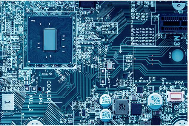
2. PCBA assembly process design, PCBA assembly process design, that is, the component layout structure of the components on the front and back of the PCB. It determines the process PCB factory method and path during assembly, so it is also called process path design.
3. Component layout design, component layout design, that is, the position, direction and spacing design of components on the assembly surface. The layout of components depends on the welding method used, and the placement of components for each welding method, The direction and spacing have specific requirements, so this book introduces the layout design requirements according to the welding process used in the package.

It should be pointed out that sometimes an assembly surface needs two or more welding processes, such as "reflow welding ten" For this type of situation, PCBA should be designed according to the soldering process used by each package.
4. Assembly process design, assembly process design, that is, design for soldering through rate, through the matching design of pads, solder mask and stencil, to achieve quantitative and stable distribution of solder paste, and through layout design. The simultaneous melting and solidification of all solder joints of a single package, through the reasonable connection design of the mounting holes, to achieve a tin penetration rate of 75%, etc., these design goals are ultimately to improve the welding yield.
There are many contents of the thermal design of PCBA, and the specific requirements of each PCB circuit board content will have some differences. For example, if the thermal design of the heat sink pad appears less tin, we can use some methods to solve it, the most common is to increase Cooling holes. So when we encounter some problems, we don’t need to panic. Find some professional people to solve all our problems.
(1) Thermal design of heat sink pad. In the soldering of heat sink components, there will be less tin in the heat sink pad. This is a typical application that can be improved by heat sink design.
For the above situation, the chip factory can use the method of increasing the heat capacity of the heat dissipation hole to design. Connect the heat dissipation hole to the inner ground layer. If the ground layer is less than 6 layers, it can isolate a part from the signal layer as a heat dissipation layer while reducing the aperture To the smallest available aperture size...
(2) PCBA thermal design of high-power ground jack.
In some special PCBA product design, the insertion hole sometimes needs to be connected to multiple ground/electric plane layers. Because the contact time between the pin and the tin wave during wave soldering is very short, it is often 2~3s. The heat capacity of the hole is relatively large, and the temperature of the lead may not meet the welding requirements, forming a cold solder joint.