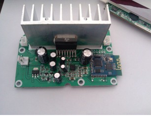
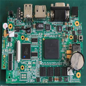
Some companies do not manage documents well. Even the most basic circuit board (PCB) files are missing. For the smooth transfer of products, the following introduces the basic files that should be available for general circuit board assembly (PCBA) transfer.
1. Gerber file or PCB CAD file Gerber-file
Gerber file is the most basic PCB circuit board manufacturing file. After the PCB factory receives the Gerber file and imports it into the CAM software, it can provide production data for each PCB process. Gerber data can also provide image data for specific equipment, Such as automated optical inspection equipment (AOI), can also be used to define the basis of PCB steel plate aperture (aperture).
2.Fab drawing (manufacturing standard)
fab drawing
This specification generally requires the PCB manufacturer to complete a circuit board, so the above usually contains the following information. The circuit board assembly factory usually uses this specification as the basis for inspection when inspecting the incoming materials:
The color of the insulating printing ink. It is generally green, but there are also black and red.
Screen printing ink color. It is generally white, but also yellow, and other colors are rare.
Surface Finished of the printed circuit board, such as ENIG, HASL, OSP... etc. Some ENIGs also specify the thickness of the gold layer and the nickel layer, and some even specify the thickness of the copper foil.

The substrate grade of the circuit board. The current circuit boards are divided into lead-free and lead-free processes. The temperature resistance requirements of the lead-free process are relatively high. When necessary, it is best to specify the Tg value (lead-free 150C or more) and Td value (lead-free 325C) of the FR4 substrate. Above), Z-axis expansion coefficient (300ppm/degree or less).
Electrical properties of copper foil. Especially high-frequency products.
V-cut and additional machining or drilling information.
Jigsaw style and size.
3. Panel drawing (Jigsaw/Connected board specifications)
Coupling specifications
The above Gerber document only defines the data of a single-chip PCB. However, in order to improve the utilization rate of the circuit board and the efficiency of the manufacturing plant, the actual output of the circuit board is designed by the board/connected board. The shape of the board is, The style and size will affect the design of the following tools, and different jigsaw methods will even make the original tools unusable:
Steel plate (Stencil)
Vacuum block
Parts Visual Inspection template (Visual Inspection template)
MDA (Manufacturing Defect Analyzer) or ICT (In-Circuit Tester) test fixture
FVT (Function Verification Tester, function test fixture)
When transferring between different production lines and different factories, remember to use the original jigsaw style. If the original file does not define the jigsaw style, you can request it from the original circuit board manufacturer and then standardize it.
4. Placement Component X-Y table (XY coordinates of SMT parts)
SMT part XY coordinates
The SMT printing machine determines the position of the part to be placed on the circuit board according to the X, Y coordinate axes defined by the user. Of course, there are other parameters (Z axis, rotation...) to form the SMT printing machine. As long as the circuit board designer can generate a table of X and Y coordinates of the part through PCB CAD, it can greatly reduce the time for SMT engineers to write the program.
If there is no way to generate X, Y coordinate tables from PCB CAD, you can still use the traditional method to slowly measure out one part by one part with the projector, or open the Gerger file and measure it on the computer. However, no matter which method is used to measure the result, it is actually necessary to fine-tune the SMT machine to match the actual coordinates.
5. Readible plots file (readable circuit board layer)
Readable circuit board layer
Most people may not be able to directly read Gerber's files. Generally, we will output each layer of the PCB into a readable PDF document, including solder paste layer, silk screen layer, shielding layer and various circuit layers.