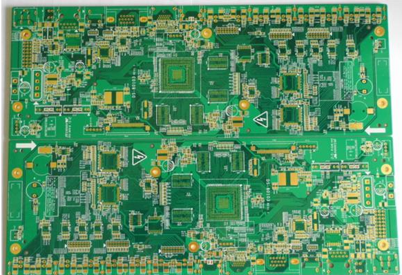
PCBA needs to be tested before use. It can only be used if it passes the test, and it cannot be used if it fails. However, there are many issues to consider when PCBA is tested. First of all, everyone should know the main content of PCBA, so what are the basic content of PCBA when testing.
1, ICT test mainly includes circuit on-off, voltage and current values and fluctuation curves, amplitude, noise, etc...
2, FCT testing requires IC program firing, simulates the function of the entire PCBA board, finds problems in the hardware and software, and is equipped with necessary production fixtures and test racks.
3, the fatigue test is mainly to sample the PCBA board of the PCB factory, and perform high-frequency, long-term operation of the function, observe whether there is failure, and judge the probability of failure in the test, so as to feedback the working performance of the PCBA board in the electronic product.
4, the test in harsh environments is mainly to expose the PCBA board to extreme temperature, humidity, drop, splashing, and vibration, and obtain the test results of random samples, thereby inferring the reliability of the entire PCBA board batch product.

5, the aging test is mainly to energize the PCBA board and electronic products for a long time, keep them working and observe whether there are any failures. After the aging test, the electronic products can be sold in batches.
PCBA welding and heating process often produce a larger temperature difference than PCBA. Once this temperature difference exceeds the standard, it will cause poor soldering, so we must control this temperature difference during operation. The thermal design of PCBA is constructed by many parts, and each part has different functions.
If the temperature difference is relatively large, it will also cause poor soldering, such as the opening of the QFP pin, the rope suction, the tombstone of the chip component, the displacement, and the shrinkage and fracture of the BGA solder joint. We can solve some problems by changing the heat capacity. problem..
(1) Thermal design of heat sink pad. In the soldering of heat sink components, there will be less tin in the heat sink pad. This is a typical application that can be improved by heat sink design.
For the above situation, PCB circuit board can be designed by increasing the heat capacity of the heat dissipation hole. Connect the heat dissipation hole to the inner ground layer. If the ground layer is less than 6 layers, you can isolate a part from the signal layer as a heat dissipation layer while reducing the aperture Reduce to the smallest available aperture size.
(2) The thermal design of the high-power ground jack. In some special product designs, the insertion hole sometimes needs to be connected to multiple ground/electric plane layers. Because the contact time between the pin and the tin wave during wave soldering is the soldering time Very short, usually 2~3s. If the heat capacity of the socket is relatively large, the temperature of the lead may not meet the welding requirements, and a cold solder joint will be formed.
In order to avoid this situation, a design called star-moon hole is used, which separates the welding hole of the chip factory from the ground layer, and realizes the large current through the power hole.
(3) In the thermal design of BGA solder joints, there will be a unique phenomenon of "shrinkage fracture" due to unidirectional solidification of solder joints under the mixed assembly process conditions. The root cause of this defect is the mixed assembly process itself. Characteristics, but can be improved by slow cooling through the optimized design of the BGA corner wiring.
According to the experience provided by the above PCBA process cases, the solder joints that generally undergo shrinkage and fracture are located at the corners of the BGA. It can be avoided by increasing the heat capacity of the BGA corner solder joints or reducing the heat transfer speed to synchronize it with other solder joints or post-cooling. The phenomenon that it is pulled off under the BGA warping stress due to the first cooling occurs.