a. In the PCB printing process, due to the offset between the template and the pad, the solder paste flows out of the pad. "
a. Follow up whether the pads, component pins and solder paste are oxidized. /
b. Adjust the precise alignment of the template opening and the pad.
During component mounting, solder paste is placed between the lead and the pad of the chip component. If the pad and the component lead are poorly wetted (poor solderability), the liquid solder will shrink and cause soldering. Insufficient seam, all solder particles cannot aggregate into a solder joint.
Part of the liquid solder will flow out of the solder joint and form tin beads. "
b. Excessive pressure on the Z axis during the placement process will squeeze the solder paste out of the pad.
B. Accurately adjust the Z axis pressure.
C. The heating speed is too fast, and the time is too short. The internal moisture and solvent of the solder paste cannot be completely volatilized. When it reaches the reflow soldering area, the solvent and moisture will boil and the tin beads will splash out. d. Adjust the temperature rise rate of the activation zone in the preheating zone.
D. The opening size and outline of the template are not clear. "E. Check whether the opening and outline of the template are clear, and replace the template if necessary."
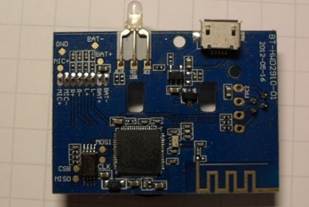
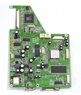
Frequently Asked Questions of SMT Chip Processing Factory

Tombstone (Manhattan phenomenon), a. Due to uneven heating at both ends of the component, or the width and length of the two ends of the pad and the excessively large gap, the solder paste is melted sequentially. a. The components are uniform and reasonably designed to be symmetrical in size at both ends of the pad. One end of the component is soldered to the pad and the other end is upright.
b. The placement of the components is shifted. b. Adjust the printing parameters and placement position.
c. The flux in the solder paste makes the component float. "C. Use a flux with a moderate amount of solder (the lead-free solder paste flux is 10.5±0.5%)." d. The solderability of the component is poor. d. Use lead-free solder paste or solder paste containing silver and bismuth without materials. E. The thickness of the printed solder paste is not enough. " E. Increase the printing thickness. That is, change the partial stencil thickness (conventional stencil thickness 0.1 0.12 0.15) mm"
"Bridge (disconnected solder joints are connected one after another),"
"A. Solder paste quality problem, the metal content in the solder paste is too high
And printing time is too long. "A. Replace or add new solder paste (new solder paste can be added regularly during the printing process to maintain its metal content and viscosity) One of the most common defects in SMT production, it will cause short circuits between components.
b. There is too much solder paste, low viscosity, and poor slump. After preheating, it overflows to the outside of the pad, leading to bridging of the solder joints with tighter gaps. b. Reduce the squeegee pressure and use solder paste with a viscosity of 190±30Pa·S.
"C. Inaccurate printing registration or excessive printing pressure can easily cause fine-pitch QFP bridging." c. Adjust the template for precise registration. d. Excessive pressure on the placement of components, the solder paste overflows after being pressed. D. Adjust the Z axis pressure. e. The chain speed and heating speed are too fast, and the solvent in the solder paste is too late to volatilize. "E. Adjust the reflow temperature curve, and adjust the chain speed and furnace temperature according to the actual situation."
Formation and solutions of common problems in SMT chip processing plants
"Less solder joints, insufficient amount of solder" "a. Insufficient solder paste, printing after the machine stops, the opening of the stencil is blocked, and the quality of the solder paste deteriorates." a. Increase the thickness of the template, increase the printing pressure, and check after the machine is shut down. Whether the template is blocked. The template opening used for lead solder should be ≥100% larger than the pad if the design permits.
b. The solderability of pads and components is poor. b. Use pads and components with better solderability.
c. Less reflow time. c. Increase the reflux time, that is, adjust the speed of the reflux chain
False soldering a. The solderability of components and pads is poor. a. Strengthen the screening of PCB and components to ensure good soldering performance.
b. Improper reflow soldering temperature and heating speed. b. Adjust the reflow soldering temperature curve.
c. The printing parameters are incorrect. c. Change the pressure and speed of the squeegee to ensure a good printing effect.
d. The stagnation time after printing is too long, and the activity of the solder paste becomes poor. d. After the solder paste is printed, it should be reflow soldered as soon as possible.
Cold welding a. The heating temperature is not suitable.A. Adjust the reflow temperature curve, according to the curve reference provided by the supplier, and then adjust it according to the actual situation of the product produced. "The surface of the solder joint is dark and rough, and there is no fusion with the welded object."
B. Solder deterioration. b. Replace with new solder paste. c. The preheating time is too long or the temperature is too high. c. Check whether the equipment is normal and correct the preheating conditions.
Wicking phenomenon " wicking phenomenon is generally considered to be the component pin
The thermal conductivity is large, and the temperature rises rapidly so that the solder preferentially wets the pins. The wetting force between the solder and the pin is much greater than the wetting force between the solder and the pad. The upturn of the pin will aggravate the wicking phenomenon. happen. In infrared reflow soldering, the organic flux in the PCB substrate and solder is an excellent absorption medium for infrared rays, while the pins can partially reflect infrared rays. In contrast, the solder preferentially melts, and its wetting power with the pad It is greater than the wetting force between the solder and it and the pin, so the solder will not climb up the pin, on the contrary the solder will climb up the pin. During reflow soldering, the SMA should be fully preheated and then placed in the reflow oven to carefully check and ensure the solderability of the PCB board pads; the coplanarity of the soldered components cannot be ignored, and the devices with poor commonality should not be ignored. Used in production. IC pin open circuit / virtual soldering "a. Poor coplanarity of components, especially QFP devices, due to improper storage, resulting in pin deformation, sometimes difficult to find (some mounters do not have coplanarity check function). "Confirm the quality of the material" "The false soldering of some pins after the IC pins are soldered is a common soldering defect." "
b. The solderability of the pins is not good, the pins are yellow, and the storage time is long. Confirm material quality
"C. The activity of the solder paste is not enough and the metal content is low,
The solder paste usually used for soldering of QFP devices has a metal content of not less than 90%. Fourth, the preheating temperature is too high, causing oxidation of the parts and poor solderability. Fifth, the size of the template opening is small and the amount of tin is not enough, and corresponding solutions are made for the above problems. "1. Adjust the reflow soldering temperature curve. 2. Expand the stencil opening by 0.05
Solder beading a. The thickness of the printed circuit is too high; the solder joints and components overlap too much. is to change the shape of the pores of the template so that there is less solder paste between the low-foot components and the solder joints. Solder beading is a special phenomenon of solder balling when using solder paste and SMT process. Simply put, solder beading refers to those very large solder balls with (or no) small solder balls attached to them. It is formed around components with extremely low feet, such as chip capacitors. Solder beading is caused by flux exhaust. In the preheating stage, this exhaustion exceeds the cohesion of the flux. The exhaust promotes the formation of stand-alone pellets of solder paste under low-gap components, which melts the solder paste during reflow. Come out from under the element again, and coalesce.